A
B
C
D
Text Solution
Verified by Experts
The correct Answer is:


Topper's Solved these Questions
SEMICONDUCTORS
MHTCET PREVIOUS YEAR PAPERS AND PRACTICE PAPERS|Exercise Exercise 1 ( TOPICAL PROBLEMS )|84 VideosSEMICONDUCTORS
MHTCET PREVIOUS YEAR PAPERS AND PRACTICE PAPERS|Exercise Exercise 1 ( MISCELLANEOUS PROBLEMS )|33 VideosSCALARS AND VECTORS
MHTCET PREVIOUS YEAR PAPERS AND PRACTICE PAPERS|Exercise Exercise 2 (Miscellaneous Problems)|20 VideosSTATIONARY WAVES
MHTCET PREVIOUS YEAR PAPERS AND PRACTICE PAPERS|Exercise MHT CET Corner|28 Videos
Similar Questions
Explore conceptually related problems
MHTCET PREVIOUS YEAR PAPERS AND PRACTICE PAPERS-SEMICONDUCTORS-MHT CET Corner
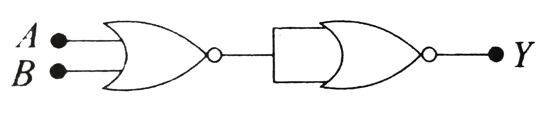
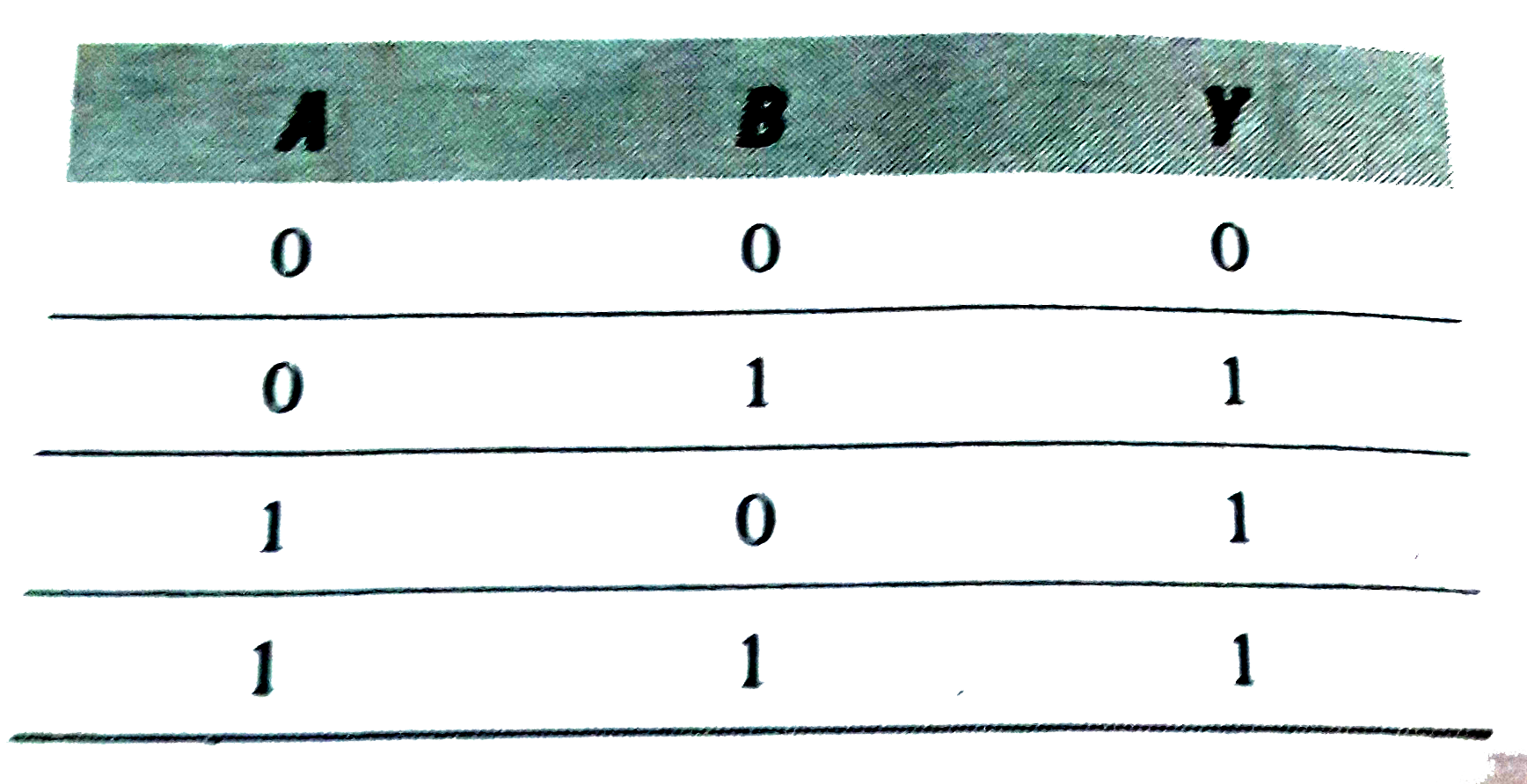
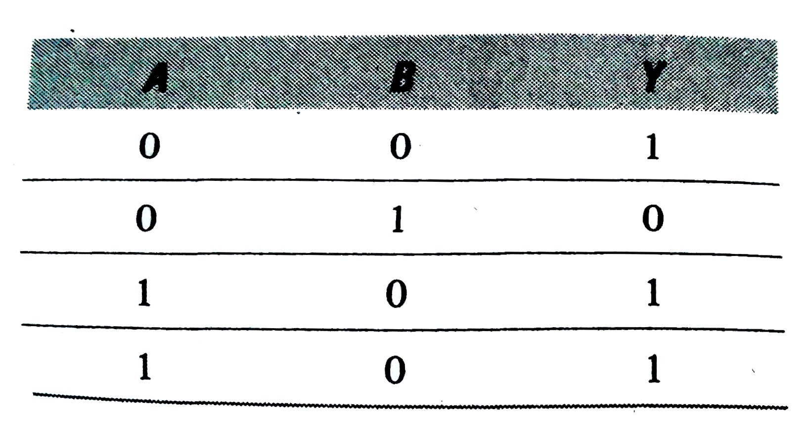
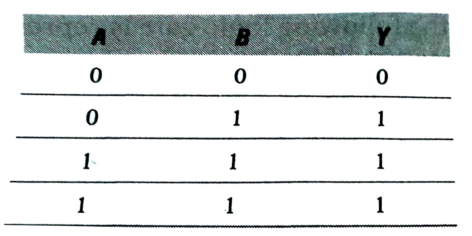
- In the following circuit, the output Y for all possible inputs A and B...
Text Solution
|
- The schematic symbol of light emitting diode (LED) is
Text Solution
|
- In an oscillator, for sustained oscillations, Barkhausen criterion is ...
Text Solution
|
- Which logic gate produces LOW output when any of the inputs in HIGH
Text Solution
|
- For a transitor the current ratio alpha(DC) is 69/70 the current ga...
Text Solution
|
- In insulators (CB is conduction band and VB is valence band )
Text Solution
|
- In common base circuit of a transistor , current amplification factor ...
Text Solution
|
- In a n-type semiconductor, which of the following statement is true?
Text Solution
|
- In a common emitter (CE) amplifier having a voltage gain G, the transi...
Text Solution
|
- The output (X) of the logic circuit shown in figure will be
Text Solution
|
- How does the width of the depletion layer of a p-n junction diode chan...
Text Solution
|
- To use a transistor as an amplifier
Text Solution
|
- How many NAND gates are required to realise (i) OR gates and (ii) AND ...
Text Solution
|
- LED is a p-n junction diode which is
Text Solution
|
- A p-n photodiode is made of a material with a band gap of 2.0 eV. The ...
Text Solution
|
- In diode, when there is saturation current, the plate resistance (r(p)...
Text Solution
|
- If a full wave rectifier circuit is operating from 50 Hz mains, the fu...
Text Solution
|
- The depletion layer in diode is 1 mum wide and the knee potential is 0...
Text Solution
|
- Which of the following is correct, about doping in a transistor ?
Text Solution
|
- Freuency of given AC signal is 50 Hz. When it connected to a half - wa...
Text Solution
|
- In p-type semiconductor, the major charge carriers are:
Text Solution
|