Text Solution
Verified by Experts


Topper's Solved these Questions
SEMICONDUCTOR ELECTRONICS : MATERIALS , DEVICES , AND SIMPLE CIRCUITS
VIKRAM PUBLICATION ( ANDHRA PUBLICATION)|Exercise SHORT ANSWER QUESTIONS|16 VideosSEMICONDUCTOR ELECTRONICS : MATERIALS , DEVICES , AND SIMPLE CIRCUITS
VIKRAM PUBLICATION ( ANDHRA PUBLICATION)|Exercise LONG ANSWER QUESTIONS|7 VideosSEMICONDUCTOR ELECTRONICS : MATERIALS , DEVICES , AND SIMPLE CIRCUITS
VIKRAM PUBLICATION ( ANDHRA PUBLICATION)|Exercise PROBLEMS|4 VideosRAY OPTICAL AND INSTRUMENTS
VIKRAM PUBLICATION ( ANDHRA PUBLICATION)|Exercise TEXTUAL EXERCISES|60 VideosTELANGANA MARCH-2019
VIKRAM PUBLICATION ( ANDHRA PUBLICATION)|Exercise SECTION -B|5 Videos
Similar Questions
Explore conceptually related problems
VIKRAM PUBLICATION ( ANDHRA PUBLICATION)-SEMICONDUCTOR ELECTRONICS : MATERIALS , DEVICES , AND SIMPLE CIRCUITS -VERY SHORT ANSWER QUESTIONS
- What is an n-type semiconductor ? What are the majority and minority c...
Text Solution
|
- What are intrisic and extrinsic semiconductors ?
Text Solution
|
- What is a p-type semiconductor ? What are the majority and minority ...
Text Solution
|
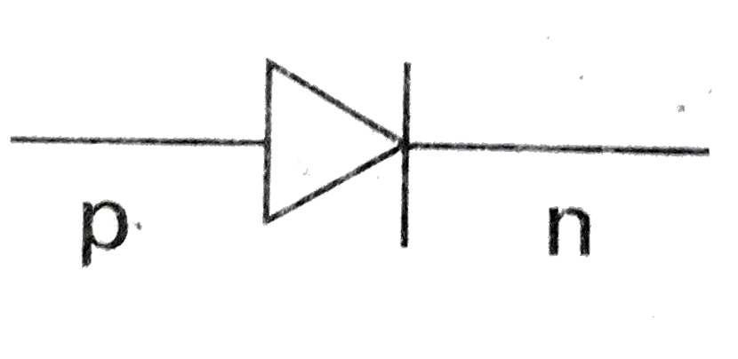
- What is p-n junction diode ? Define depletion layer.
Text Solution
|
- How is a battery connected to a junction dioide in (i) forward and (ii...
Text Solution
|
- What is the maximum percentage of rectification in half wave and ful...
Text Solution
|
- What is Zener voltage ( V(2)) and how will a Zener diode be connected ...
Text Solution
|
- Write the expressions for the efficiency of a full wave rectifier and...
Text Solution
|
- What happens to the width of depletion layer of a p-n junction when it...
Text Solution
|
- Draw the circuit symbols for p-n-p and n-p-n transistors
Text Solution
|
- Define amplifier and amplification factor.
Text Solution
|
- In which bias can be a Zener diode be used as voltage regulator ?
Text Solution
|
- Which gates are called universal gates?
Text Solution
|
- Write the truth table of NAND gate. How does it differ from AND gate?
Text Solution
|