Text Solution
Verified by Experts


Topper's Solved these Questions
SEMICONDUCTOR ELECTRONICS : MATERIALS , DEVICES , AND SIMPLE CIRCUITS
VIKRAM PUBLICATION ( ANDHRA PUBLICATION)|Exercise TEXTUAL EXERCISES|11 VideosRAY OPTICAL AND INSTRUMENTS
VIKRAM PUBLICATION ( ANDHRA PUBLICATION)|Exercise TEXTUAL EXERCISES|60 VideosTELANGANA MARCH-2019
VIKRAM PUBLICATION ( ANDHRA PUBLICATION)|Exercise SECTION -B|5 Videos
Similar Questions
Explore conceptually related problems
VIKRAM PUBLICATION ( ANDHRA PUBLICATION)-SEMICONDUCTOR ELECTRONICS : MATERIALS , DEVICES , AND SIMPLE CIRCUITS -ADDITIONAL EXERCISES
- The Number of silicon atoms per m^(3) is 5 xx 10^(28) . This is doped ...
Text Solution
|
- In an intrinsic semiconductor the energy gapE(g ) is1.2 eV. Its hole ...
Text Solution
|
- In a p-n junction diode, the currentI can be expressed as I=I(0)exp ((...
Text Solution
|
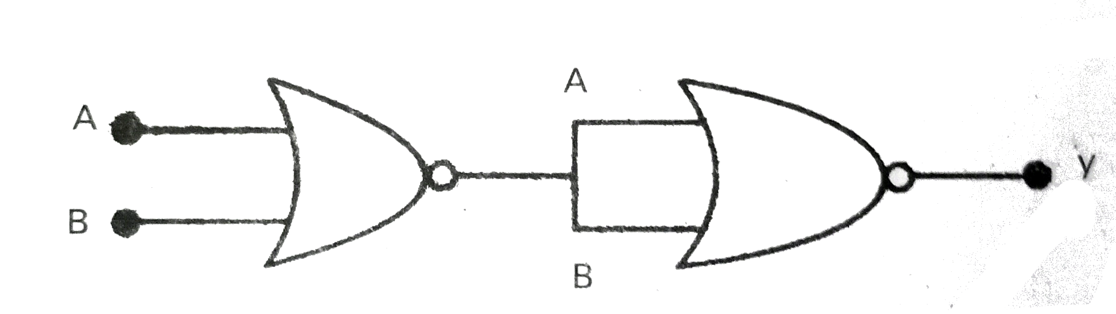
- You are given the two circuit as shown in figure, show that the circui...
Text Solution
|
- Write the truth table for a NAND gate connected as given in figure. ...
Text Solution
|
- You are given two circuits as shown in figure, which consists of NAND ...
Text Solution
|
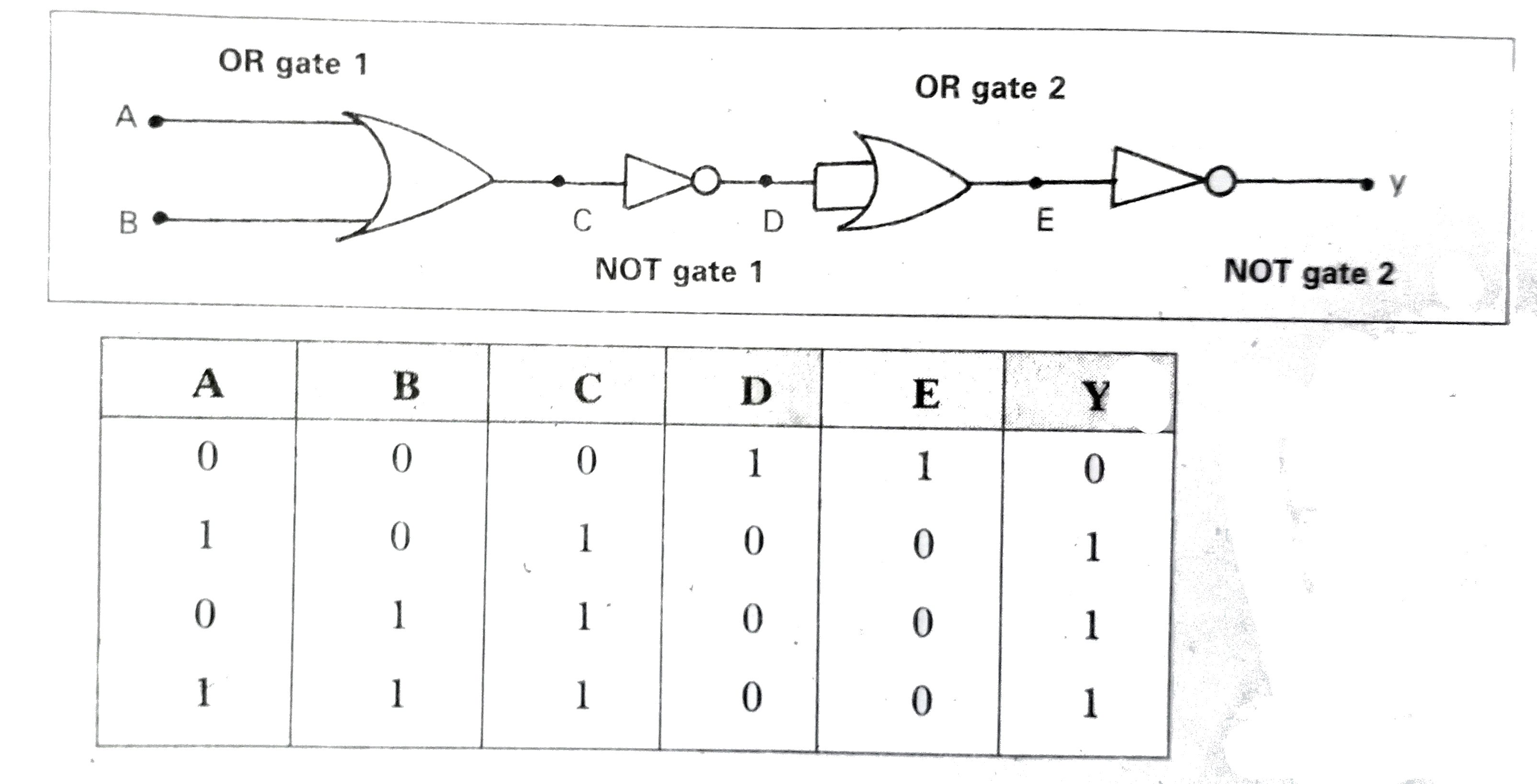
- Write the truth table for circuit given in figure, below consisting of...
Text Solution
|
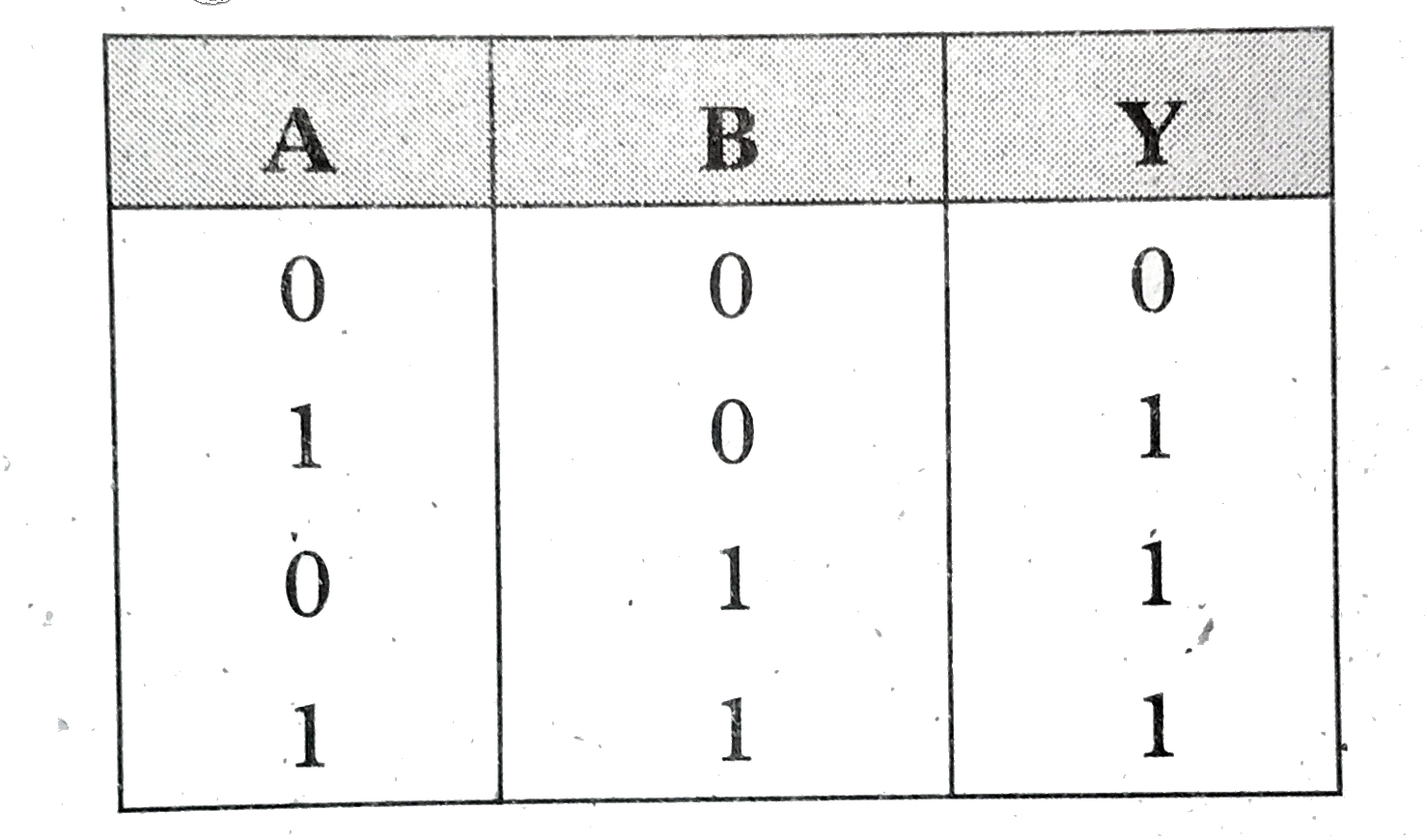
- Write the truth table for the circuits given in figure, consisting of ...
Text Solution
|