If the input terminals of NAND gate are joined togather we get NOT gate. Now if the input A and B are inverted by using two NOT gates (obtained from NAND gates) and their outputs are jointly fed to the NAND gate as shown in Fig.9.35, we get the arrangement which works as OR gate.
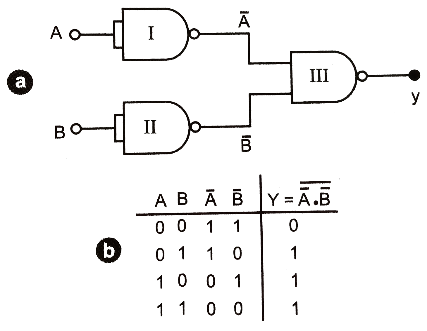
Explaination. The output of gate I is,
`y_(1)=bar(A.A)=barA+barA=barA`
The output of gate II is,
`y_(2)=bar(B.B)=barB+barB=barB`
The output of gate III is,
`y=bar(y_(1).y_(2))=bar(barA.barB)=bar(barA) +bar(barB)=A+B`
As `y=A+B`, is the Boolean expression for OR gate, thus the combination works as OR gate. The truth table of the arrangement is shown in.


