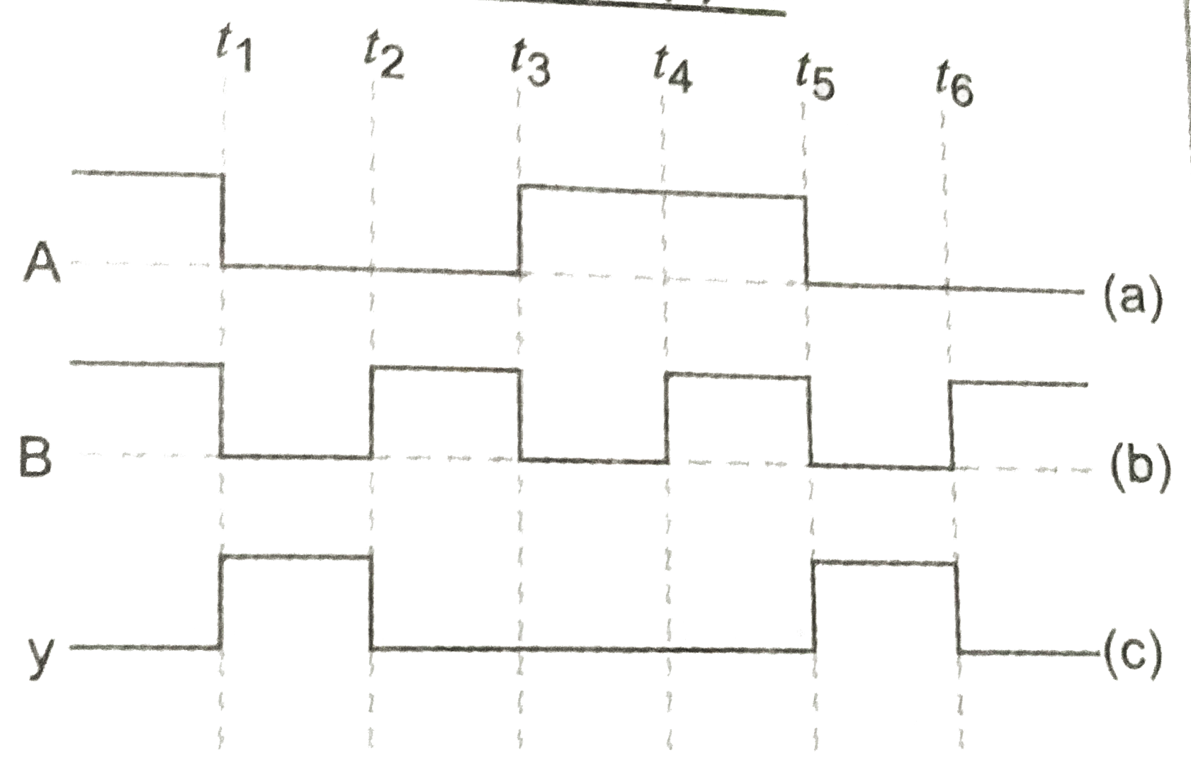
Sketch the output y from a NOR gate having input A and B as given in Fig.
Text Solution
Verified by Experts
For NOR gate the Boolean expression is `bar(A+B)=y` For the given wave form, we have the following value for A, B and y. For time `t lt t_(1), A=1, B=1` hencey `=0` For time `t_(1) "to" t_(2), A=0, B=0` hencey `=1` For time `t_(2) "to" t_(3), A=0, B=1` hencey `=0` For time `t_(3) "to" t_(4), A=1, B=0` hencey `=0` For time `t_(4) "to" t_(5), A=1, B=1` hencey `=0` For time `t_(5) "to" t_(6), A=0, B=0` hencey `=1` For time `t gt t_(6), A=0, B=1` hencey `=0` The wave from for output y is as shown in Fig.
Topper's Solved these Questions
ELECTRONIC DEVICES
PRADEEP|Exercise SAMPLE PROBLEM|2 Videos
ELECTRONIC DEVICES
PRADEEP|Exercise CONCEPTUAL PROBLEMS|1 Videos
ELECTROMAGNETIC WAVES
PRADEEP|Exercise II Focus multiple choice question|5 Videos
ELECTROSTATICS
PRADEEP|Exercise ASSERTION-REASON TYPE QUESTIONS|2 Videos
Similar Questions
Explore conceptually related problems
Sketch the output Y from NAND gate having input A A and B given below, Fig.
Justify the output wavefrom (y) of the OR gate for input and as gives in Fig.
Sketch the output waveform Y from a NAND gate having following inputs A and B
Sketch the output wavefrom Y from a NAND gate having following inputs A and B
A student has to use an appropriate number of (i) NAND gates (only) to get the output y_(1) (ii) NOR gates (only) to get the output y_(2) from two given input A and B as shown in the Fig. Identify the 'equivalent gate' needed in each case. Show how one can connect an appropriate number of (i) NAND (ii) NOR gates respectively in the two cases to gat the equivalent gates.
Find the Boolean expression of the output y in terms of the input A and B for the circuit shown in Fig.Name the gate formed.
Write the output waveform of the OR gate for the inputs