


Topper's Solved these Questions
ELECTRONIC DEVICES
PRADEEP|Exercise LONG QUESTION ANSWER|2 VideosELECTRONIC DEVICES
PRADEEP|Exercise PROBLEMS FOR PRACTICE|7 VideosELECTRONIC DEVICES
PRADEEP|Exercise HIGHER ORDER THINKING SKILLS|1 VideosELECTROMAGNETIC WAVES
PRADEEP|Exercise II Focus multiple choice question|5 VideosELECTROSTATICS
PRADEEP|Exercise ASSERTION-REASON TYPE QUESTIONS|2 Videos
Similar Questions
Explore conceptually related problems
PRADEEP-ELECTRONIC DEVICES-Exercise
- What is logic gate? Distinguish between AND and OR gates.
Text Solution
|
- What are main logic gates? How many types are they? Draw their symbols...
Text Solution
|
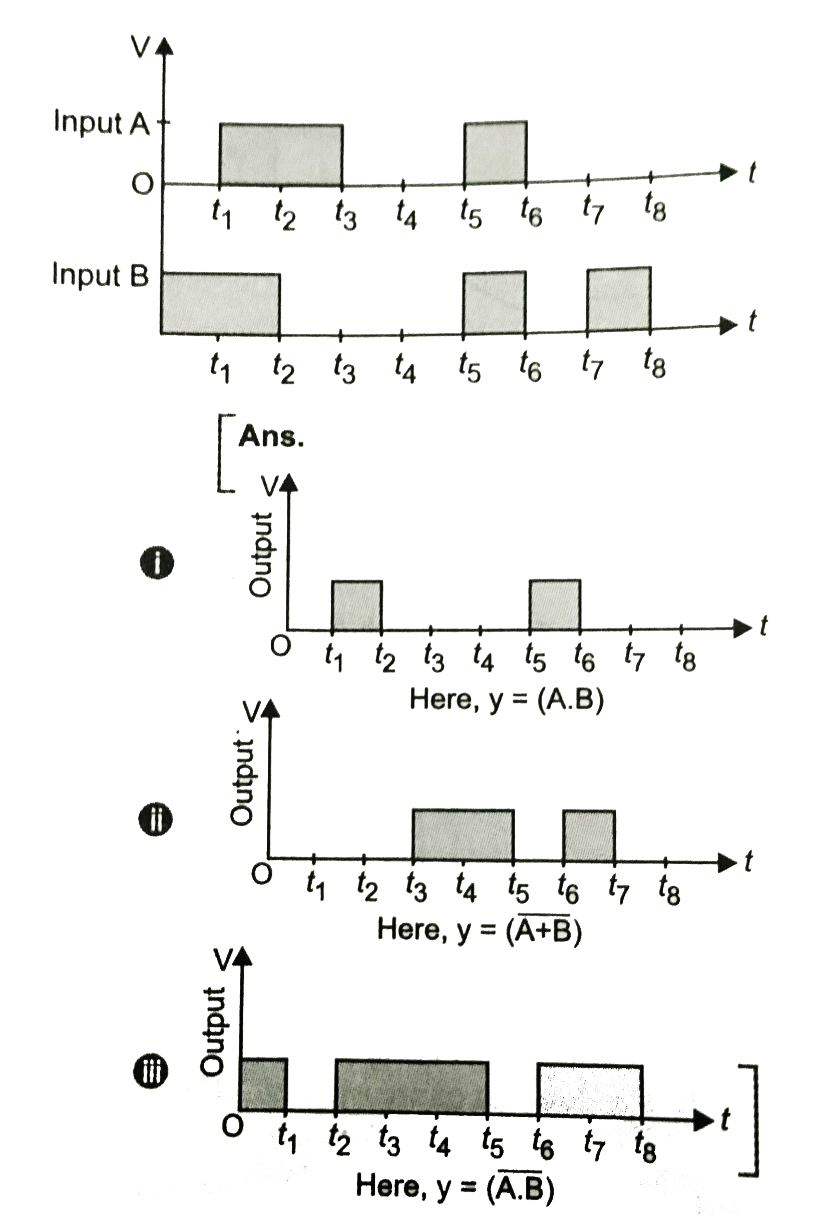
- Two signals A, B as given below are applied to (i) AND (ii) NOR and (i...
Text Solution
|
- Give the logic symbol, Boolean expression and truth table of NAND gate...
Text Solution
|
- Identify the logic gate equivalent to the circuit shown in the Fig.Dra...
Text Solution
|
- Discuss an integrated circuit. Explain the meaning of SSI, MSI, LSI an...
Text Solution
|
- What is integrated circuit ? Discuss the advantages of integrated circ...
Text Solution
|
- Explain formation of energy band in solids. Distinguish between conduc...
Text Solution
|
- Draw the "energy bands" diagram for a (i) pure semiconductor (ii) insu...
Text Solution
|
- What is an extrinsic semiconductor? Discuss the working of the various...
Text Solution
|
- Distinguish between (i) Intrinsic and Extrinsic semiconductor and (i...
Text Solution
|
- Distinguish between n-type and p-type semiconductors on the basis of e...
Text Solution
|
- Draw a circuit diagram of a full-wave rectifier. Explain its working p...
Text Solution
|
- Explain (i) forward biasing (ii) reverse biasing of a P-N junction dio...
Text Solution
|
- What is a p-n junction diode? Define the term 'dynamic resistance' for...
Text Solution
|
- What do you understand by decimal number system and binary number syst...
Text Solution
|
- What do you understand by logic gate? Why is it so called? State the t...
Text Solution
|
- Describe (i) NAND gate, (ii) NOR gate and (iii) XOR gate.
Text Solution
|
- Explain how an OR gate may be constructed with AND and NOT gates. A lo...
Text Solution
|
- A semiconductor has equal electron and hole concentration of 6xx10^(8)...
Text Solution
|