


Topper's Solved these Questions
ELECTRONIC DEVICES
PRADEEP|Exercise LONG QUESTION ANSWER|2 VideosELECTRONIC DEVICES
PRADEEP|Exercise PROBLEMS FOR PRACTICE|7 VideosELECTRONIC DEVICES
PRADEEP|Exercise HIGHER ORDER THINKING SKILLS|1 VideosELECTROMAGNETIC WAVES
PRADEEP|Exercise II Focus multiple choice question|5 VideosELECTROSTATICS
PRADEEP|Exercise ASSERTION-REASON TYPE QUESTIONS|2 Videos
Similar Questions
Explore conceptually related problems
PRADEEP-ELECTRONIC DEVICES-Exercise
- What do you understand by logic gate? Why is it so called? State the t...
Text Solution
|
- Describe (i) NAND gate, (ii) NOR gate and (iii) XOR gate.
Text Solution
|
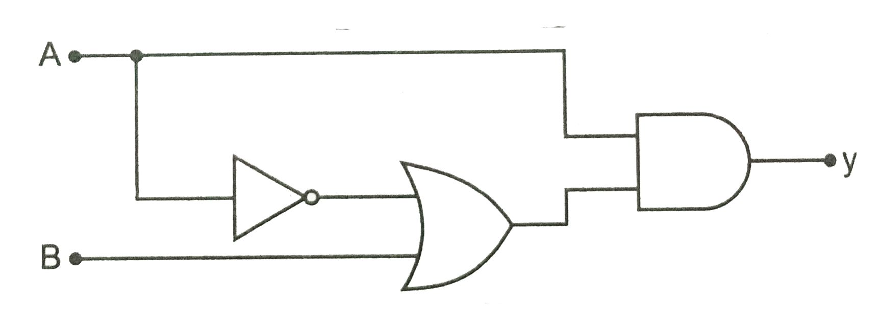
- Explain how an OR gate may be constructed with AND and NOT gates. A lo...
Text Solution
|
- A semiconductor has equal electron and hole concentration of 6xx10^(8)...
Text Solution
|
- In a pure semiconductor, the number of conduction electrons is 6xx10^(...
Text Solution
|
- A p-type semiconductor has acceptor energy level 53meV above the valen...
Text Solution
|
- The electrical conductivity of a semiconductor increases when electrom...
Text Solution
|
- A doped semiconductor has impurity levels 20 meV below the conduction ...
Text Solution
|
- Pure Si at 500K has equal number of electron (n(e)) and hole (n(h)) co...
Text Solution
|
- Find the number density of impurity atoms that must be added to a pure...
Text Solution
|
- Determine the number density of donor atoms which have to be added to ...
Text Solution
|
- On doping germanium with donor atoms of density 10^(17)cm^(-3), find i...
Text Solution
|
- The energy of a photon of sodium light wavelength 5890 Å equals the en...
Text Solution
|
- Calculate the number of states per cubic metre of sodium in 3s band. T...
Text Solution
|
- Find the current produced at room temperature in a pure germanium plat...
Text Solution
|
- If resistivity of pure silicon is 3000 Omega meter, and the electron a...
Text Solution
|
- The V-I characteristics of a silicon diode is given in Fig .Calculate ...
Text Solution
|
- A p-n junction is fabricated from a semiconductor with band gap of 3.0...
Text Solution
|
- The width of depletion region in a P-N junction diode is 500 nm and an...
Text Solution
|
- Calculate the current through the circuit and the potential difference...
Text Solution
|