Home
Class 12
PHYSICS
Input signal A and B are applied to the ...

Input signal A and B are applied to the input terminals of the 'dotted box' set up shown here. Ley y be the final output signal from the box. What are the wavefroms of the signal labelled as `C_(1)` and `C_(2)` within the box giving (in brief) the reasons for getting these wave forms. Hence draw the waveform of the final output signal y. Give reasons for your choice. Write the relation between the total output y and the input signals A and B?

Text Solution

Verified by Experts

Here gate I is NAND gate working as NOT gate, gates II and IV and AND gates, gate III is NOT gate and V is NOR gate.
Boolean expression for `C_(1)=barA`.B
Boolean expression for `C_(2)=A.barB`
`:.` Output `y=bar(C_(1)+C_(2))=bar(A.B+A.barB)`
Truth table of the circuit is given below (see ahead).
The wave forms `C_(1), C_(2)` and y are shown in Fig. below

`|{:(Time,A,B,barA,barB,C_(1)=,C_(2)=,y=),("interval",,,,,bar(A).B,A.barB,bar(C_(1)+C_(2))),("For"0 "to" 1,1,0,0,1,0,1,0),("For"1 "to"2,1,1,0,0,0,0,1),("For"2"to"3,1,1,0,0,0,0,1),("For"3"to"4,0,0,1,1,0,0,1),("For more",1,0,0,1,0,1,0),(than 4,,,,,,,):}:|`
Promotional Banner

Topper's Solved these Questions

  • ELECTRONIC DEVICES

    PRADEEP|Exercise LONG QUESTION ANSWER|2 Videos
  • ELECTRONIC DEVICES

    PRADEEP|Exercise PROBLEMS FOR PRACTICE|7 Videos
  • ELECTRONIC DEVICES

    PRADEEP|Exercise HIGHER ORDER THINKING SKILLS|1 Videos
  • ELECTROMAGNETIC WAVES

    PRADEEP|Exercise II Focus multiple choice question|5 Videos
  • ELECTROSTATICS

    PRADEEP|Exercise ASSERTION-REASON TYPE QUESTIONS|2 Videos

Similar Questions

Explore conceptually related problems

input are given as shown then output signal is-

Draw the output signals C_(1) " and " C_(2) in the given combination of gates.

Which of the following figures correctly shows the phase relation between the input signal and the output signal of triode amplifier

Write the output waveform of the OR gate for the inputs

Using the wave forms of the input A and B, draw the output waveform of the given logic circuit . Identify the logic gate obtained . Write also the truth table.

Show the output waveform of OR gate for the following input waveforms of A and B

Show the output waveform of OR gate for the following input waveforms of A and B

In a common emitter amplifier the input signal is applied across

The real time variation of input signals A & B are as shown below. If the inputs are into NAND gate, then select the output signals from the following-

PRADEEP-ELECTRONIC DEVICES-Exercise
  1. Identify the gate represented by the block diagram of Fig. Write its b...

    Text Solution

    |

  2. Write the truth table for the circuit shown in Fig. Name the gate so f...

    Text Solution

    |

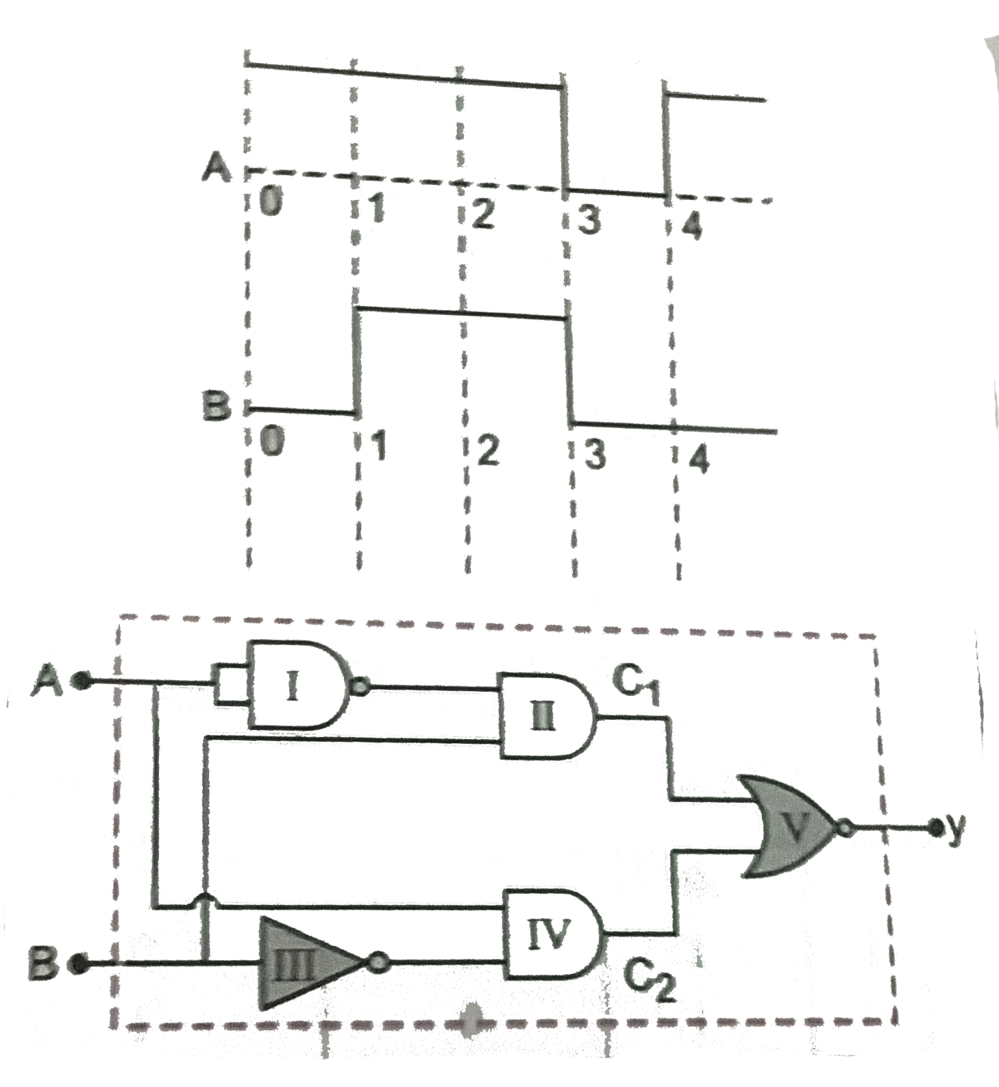
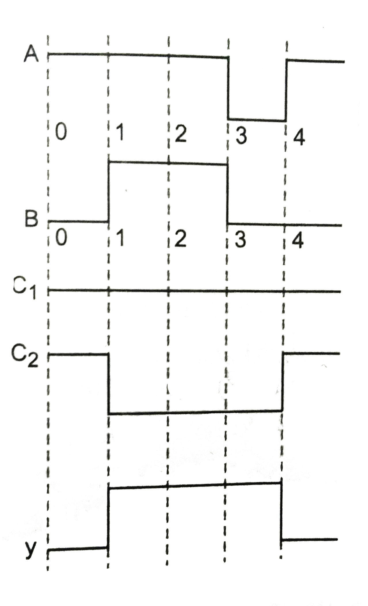
  3. Input signal A and B are applied to the input terminals of the 'dotted...

    Text Solution

    |

  4. Find the binary numbers of (32.25)(10) and (24.25)(10) and give subtra...

    Text Solution

    |

  5. The conductivity of a semiconductor increases with increase in tempera...

    Text Solution

    |

  6. In Fig . V(0) is the potential barrier across a p-n junction, when no ...

    Text Solution

    |

  7. In Fig.assuming the diode to be ideal

    Text Solution

    |

  8. A 220 V AC supply is connected between points A and B . What will be t...

    Text Solution

    |

  9. Hole is

    Text Solution

    |

  10. The output of the given circuit in Fig.

    Text Solution

    |

  11. In the circuit shown(Fig.) if the diode forward voltage drop is 0.3 V,...

    Text Solution

    |

  12. Truth table for the given circuit (Fig.)is

    Text Solution

    |

  13. When an electric field is applied across a semiconductor,

    Text Solution

    |

  14. Consider an n-p-n transistor with its base - emitter junction forward ...

    Text Solution

    |

  15. Fig.shows that transfer characteristics of a base biased CE transistor...

    Text Solution

    |

  16. In an n-p-n transistor circuit , the collector currents is 10mA . If 9...

    Text Solution

    |

  17. In the depletion region of a diode.

    Text Solution

    |

  18. What happens during regualtion action of a Zener diode?

    Text Solution

    |

  19. To reduce the ripples in rectifier circuit with capacitor filter

    Text Solution

    |

  20. The breakdown in a reverse biased p-n junction diode is more likely to...

    Text Solution

    |