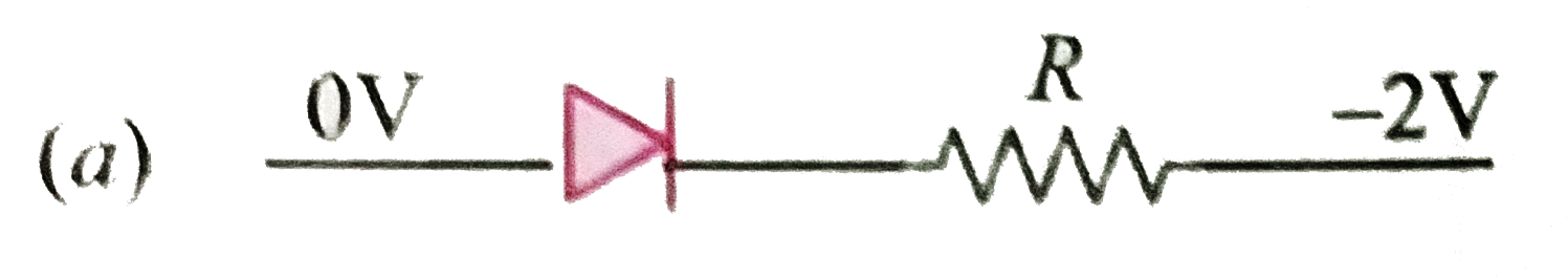
A
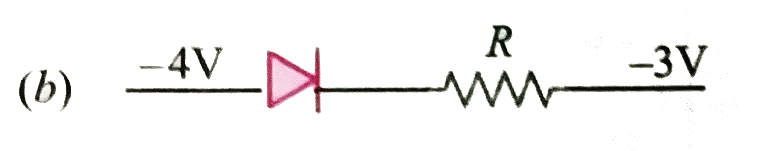
B
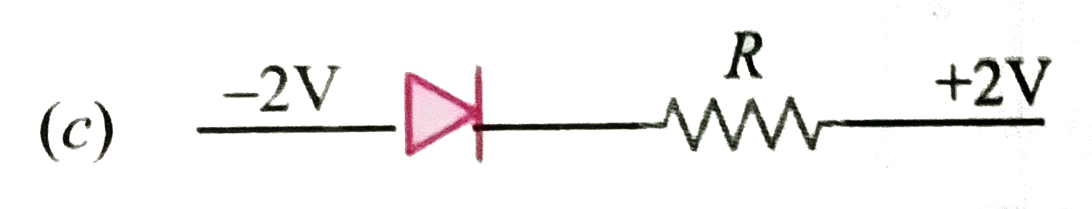
C
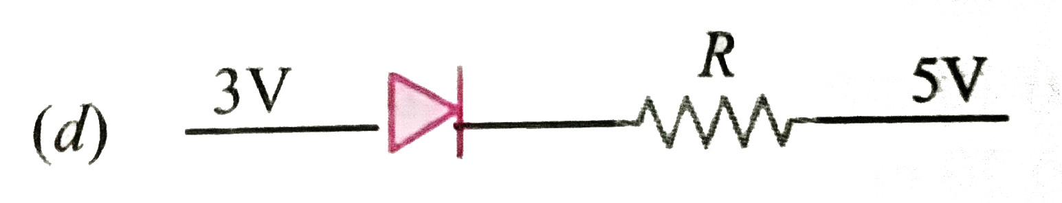
D
Text Solution
Verified by Experts
The correct Answer is:


Topper's Solved these Questions
ELECTRONIC DEVICES
PRADEEP|Exercise LONG QUESTION ANSWER|2 VideosELECTRONIC DEVICES
PRADEEP|Exercise PROBLEMS FOR PRACTICE|7 VideosELECTRONIC DEVICES
PRADEEP|Exercise HIGHER ORDER THINKING SKILLS|1 VideosELECTROMAGNETIC WAVES
PRADEEP|Exercise II Focus multiple choice question|5 VideosELECTROSTATICS
PRADEEP|Exercise ASSERTION-REASON TYPE QUESTIONS|2 Videos
PRADEEP-ELECTRONIC DEVICES-Exercise
- The dominant mechanisms for motion of charge carriers in forward and r...
Text Solution
|
- The circuit shown in figure (1) Contains two diodes each with a forwar...
Text Solution
|
- Which one of the following represents forward bias diode?
Text Solution
|
- A sinusiodal voltage of rms value 200 volt is connected to the diode a...
Text Solution
|
- In the given figure, a diode D is connected to an external resistance ...
Text Solution
|
- A diode having potential difference 0.5 V across its junction which do...
Text Solution
|
- A zener diode, having breakdown voltage equal to 15 V is used in a vol...
Text Solution
|
- The barrier potential of a p-n junction depends on : (i) type of semic...
Text Solution
|
- The number of minority carriers crossing the junction of a diode depen...
Text Solution
|
- A semiconductor X is made by dopping a germanium crystal with arsenic ...
Text Solution
|
- A full wave rectifier circuit along with the input and output are show...
Text Solution
|
- The equivalent resistance of the circuit across AB is given by .
Text Solution
|
- A p-n junction has acceptor impurity concentration of 10^(17) cm^(-3) ...
Text Solution
|
- The diode shown in the circuit is a silicon diode. The potential diffe...
Text Solution
|
- In the circuit Fig., what is the range over which the load resistance ...
Text Solution
|
- Two Zener diodes having specification 12V, 1/4W are connected in serie...
Text Solution
|
- The graph shown in Fig. represents the I-V characteristics of a zener ...
Text Solution
|
- The width of depletion region in p-n junction diode is 500 nm and an i...
Text Solution
|
- Two junction diodes, one of germanium (Ge) and other of silicon (Si) ...
Text Solution
|
- The forward biased diode connection is
Text Solution
|