Home
Class 12
PHYSICS
A semiconductor X is made by dopping a g...

A semiconductor `X` is made by dopping a germanium crystal with arsenic `(Z=33)`. A scond semiconductor `Y` is made by dopping germanium with indium `(Z=49)`. The two are joined end to end and connected to a battery as shown. Which of the following statements is correct?

A

X is P-type, Y is N-type and the junction is forward biased

B

X is N-type, Y is P-type and the junction is forward biased

C

X is P-type, Y is N-type and the junction is reverse biased

D

X is N-type, Y is P-type and the junction is reverse biased

Text Solution

Verified by Experts

The correct Answer is:
D

Arsenic has valence five and indium has valeance three. So X is N-type and Y is p-type. As positive terminal of battery is connected to N-type, and negative terminal to p-type of P-N junction, hence the junction is reverse biased.
Promotional Banner

Topper's Solved these Questions

  • ELECTRONIC DEVICES

    PRADEEP|Exercise LONG QUESTION ANSWER|2 Videos
  • ELECTRONIC DEVICES

    PRADEEP|Exercise PROBLEMS FOR PRACTICE|7 Videos
  • ELECTRONIC DEVICES

    PRADEEP|Exercise HIGHER ORDER THINKING SKILLS|1 Videos
  • ELECTROMAGNETIC WAVES

    PRADEEP|Exercise II Focus multiple choice question|5 Videos
  • ELECTROSTATICS

    PRADEEP|Exercise ASSERTION-REASON TYPE QUESTIONS|2 Videos

Similar Questions

Explore conceptually related problems

A semiconductor material x is made by doping a germanium crystal with indium another semiconductor material y is made by doping a x nad y ar then joined together and connected to a battery will the jucntion be forward or reverse biased also draw the V-I characteristics for the circuit

Sohan connects three identical bulbs X, Y and Z as shown in the figure. Which of the following statements is correct?

Two semiconductor materials X and Y shown in the given figure, are made by doping germanium crystal with indum and arsenic respectively. The two are joined end to end and connected to a battery as shown. (i). Will the junction be forward biased or reverse biased.? (ii). Sketch a V-I graph for this arrangement.

A battery and three lamps are connected as shown: Which of the following statements about the currents at X,Y and Z is correct?

A rod is made of uniform material and has non-uniform cross section. It is fixed at both the ends as shown and heated at mid-section. Which of the following are not correct?

Let P_(1):2x+y-z=3" and "P_(2):x+2y+z=2 be two planes. Then, which of the following statement(s) is (are) TRUE?

Three different gases X, Y and Z of molecular masses 2, 16 and 64 were enclosed in a vessel at constant temperature till equilbrium is reaches. Which of the following statement is correct?

PRADEEP-ELECTRONIC DEVICES-Exercise
  1. The barrier potential of a p-n junction depends on : (i) type of semic...

    Text Solution

    |

  2. The number of minority carriers crossing the junction of a diode depen...

    Text Solution

    |

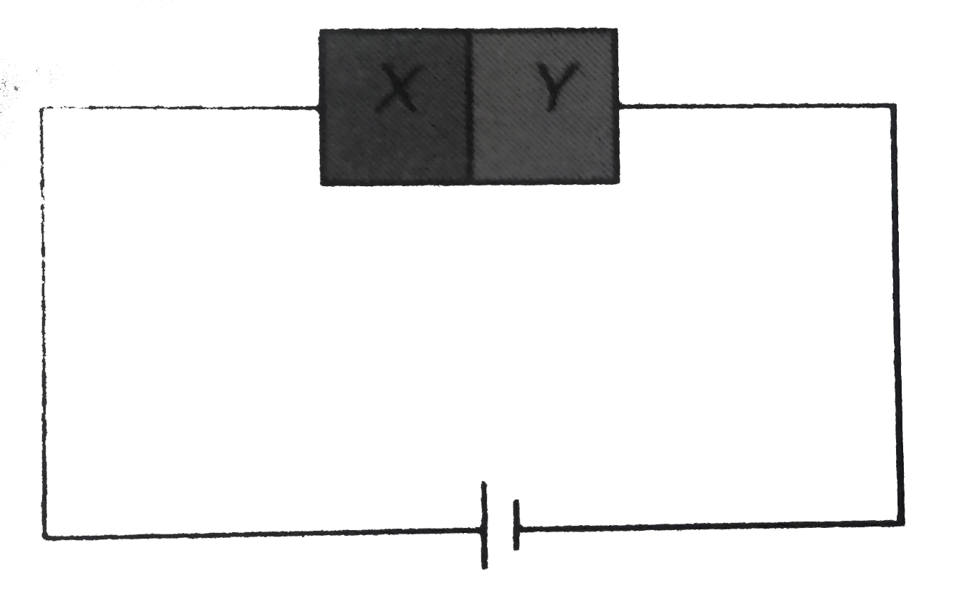
  3. A semiconductor X is made by dopping a germanium crystal with arsenic ...

    Text Solution

    |

  4. A full wave rectifier circuit along with the input and output are show...

    Text Solution

    |

  5. The equivalent resistance of the circuit across AB is given by .

    Text Solution

    |

  6. A p-n junction has acceptor impurity concentration of 10^(17) cm^(-3) ...

    Text Solution

    |

  7. The diode shown in the circuit is a silicon diode. The potential diffe...

    Text Solution

    |

  8. In the circuit Fig., what is the range over which the load resistance ...

    Text Solution

    |

  9. Two Zener diodes having specification 12V, 1/4W are connected in serie...

    Text Solution

    |

  10. The graph shown in Fig. represents the I-V characteristics of a zener ...

    Text Solution

    |

  11. The width of depletion region in p-n junction diode is 500 nm and an i...

    Text Solution

    |

  12. Two junction diodes, one of germanium (Ge) and other of silicon (Si) ...

    Text Solution

    |

  13. The forward biased diode connection is

    Text Solution

    |

  14. In the circuit, Fig.he current through the zener diode is

    Text Solution

    |

  15. The I-V characteristic of an LED is.

    Text Solution

    |

  16. The currect voltage relation of a diode is given by 1 = (e^(van v//T)...

    Text Solution

    |

  17. The given graph represents V-I characteristic for a semiconductor devi...

    Text Solution

    |

  18. For a common emiter configuration if a and beta have their usualy mean...

    Text Solution

    |

  19. The input signal given to a CE amplifier having a voltage gain of 150 ...

    Text Solution

    |

  20. The current transfer ratio beta of a transistor is 50. The input resis...

    Text Solution

    |