A
B
C
D
Text Solution
Verified by Experts
The correct Answer is:


Topper's Solved these Questions
ELECTRONIC DEVICES
PRADEEP|Exercise LONG QUESTION ANSWER|2 VideosELECTRONIC DEVICES
PRADEEP|Exercise PROBLEMS FOR PRACTICE|7 VideosELECTRONIC DEVICES
PRADEEP|Exercise HIGHER ORDER THINKING SKILLS|1 VideosELECTROMAGNETIC WAVES
PRADEEP|Exercise II Focus multiple choice question|5 VideosELECTROSTATICS
PRADEEP|Exercise ASSERTION-REASON TYPE QUESTIONS|2 Videos
Similar Questions
Explore conceptually related problems
PRADEEP-ELECTRONIC DEVICES-Exercise
- In common emitter transistor amplifier circuit, the input signal volta...
Text Solution
|
- A npn transistor is connected in common emitter configuration in a giv...
Text Solution
|
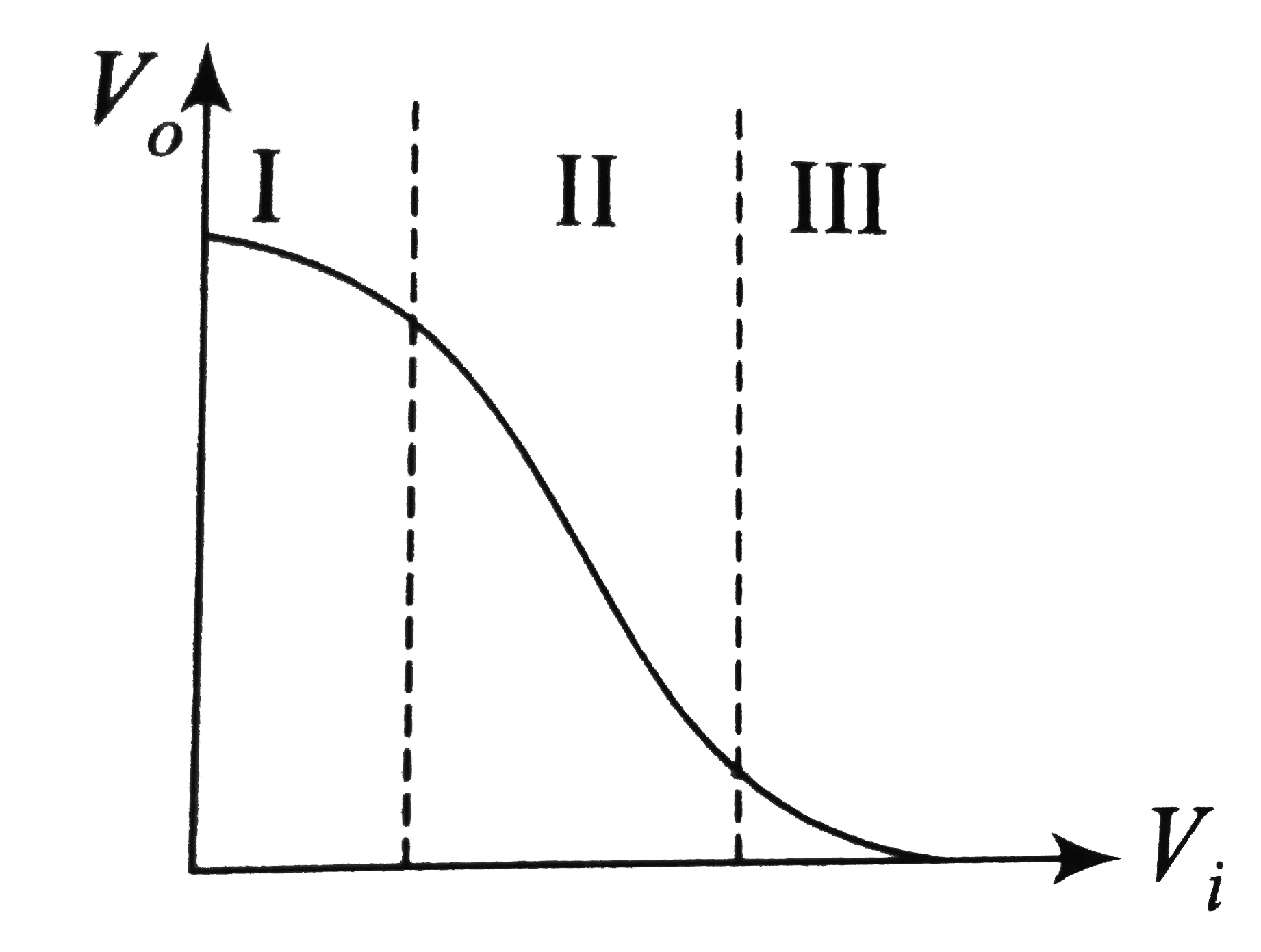
- Transfer characterstics [output voltage (V(o)) vs. input voltage (V(i)...
Text Solution
|
- In a common emitter transistor transistor amplifier, the audio signal ...
Text Solution
|
- The Boolean expression P+bar(P)Q, where P and Q are the inputs of the ...
Text Solution
|
- Which logic gate is represented by the following combination of logic ...
Text Solution
|
- If (i), (ii), (iii), (iv) are inputs to a gate and x is output, then a...
Text Solution
|
- Fig, shows a logic gate circuit with two input A and B and the output ...
Text Solution
|
- To write the decimal number 37 in binary, how many binary digit are re...
Text Solution
|
- What is the decimal number of binary number (111001.01)(2)?
Text Solution
|
- The combination of the 'NAND' gates shown here (Fig.) and (ii)) are eq...
Text Solution
|
- In the circuit Fig. the output y becomes zero for the inputs
Text Solution
|
- The Fig.shows a logic gate circuit with two inputs A and B and the out...
Text Solution
|
- The given electrical network is equivalent to:
Text Solution
|
- How many gates are required to design , y=A+barA.B ? Also name the gat...
Text Solution
|
- In the following combinations of logic gates, the outputs A, B and C a...
Text Solution
|
- To get an output y=1 from the circuit shown below, the input must be
Text Solution
|
- The following figure shows a logic gate circuit with two inputs A and ...
Text Solution
|
- The comdination of gates shown below yields
Text Solution
|
- The circuit diagram (see fig.) shows a 'logic combination' with the st...
Text Solution
|