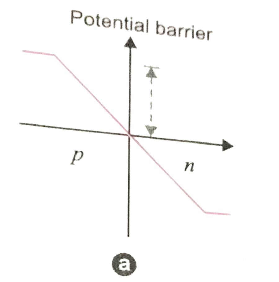
A
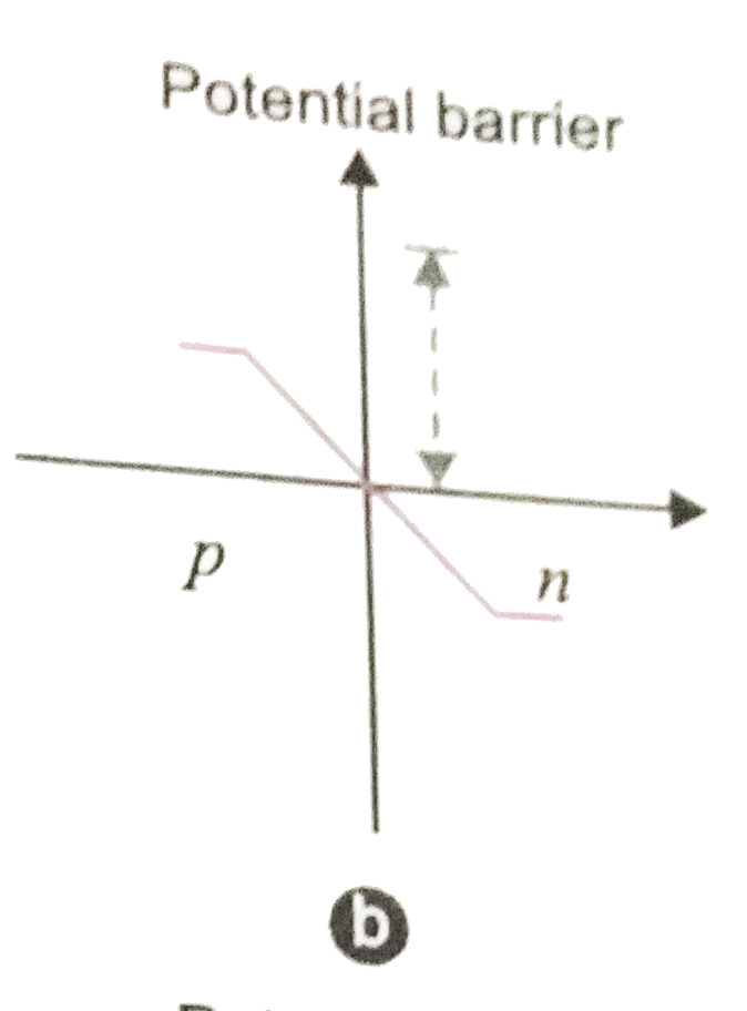
B
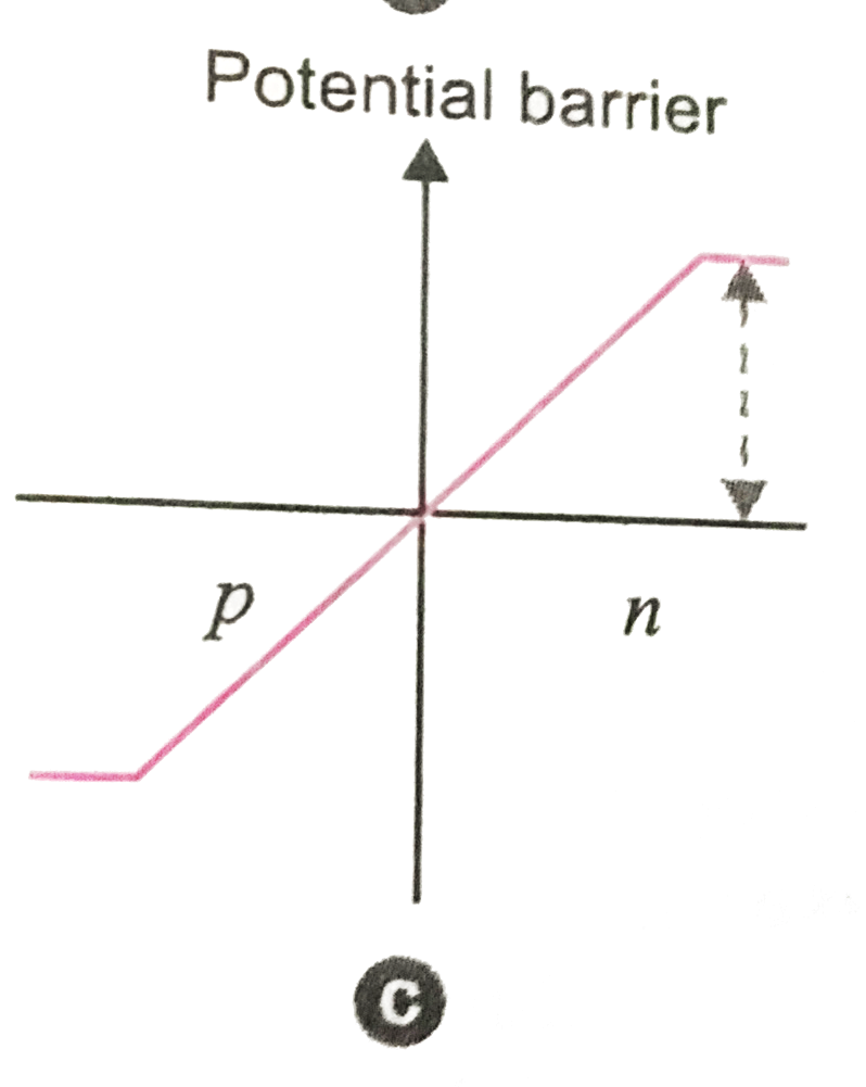
C
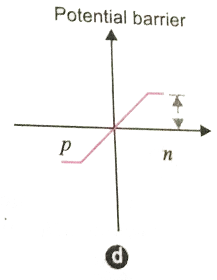
D
Text Solution
Verified by Experts
The correct Answer is:


Topper's Solved these Questions
ELECTRONIC DEVICES
PRADEEP|Exercise LONG QUESTION ANSWER|2 VideosELECTRONIC DEVICES
PRADEEP|Exercise PROBLEMS FOR PRACTICE|7 VideosELECTRONIC DEVICES
PRADEEP|Exercise HIGHER ORDER THINKING SKILLS|1 VideosELECTROMAGNETIC WAVES
PRADEEP|Exercise II Focus multiple choice question|5 VideosELECTROSTATICS
PRADEEP|Exercise ASSERTION-REASON TYPE QUESTIONS|2 Videos
Similar Questions
Explore conceptually related problems
PRADEEP-ELECTRONIC DEVICES-Exercise
- Suppose the energy liberated in the recombination of a hole-electron p...
Text Solution
|
- The forward characteristic of p-n junction is shown in Fig.What is the...
Text Solution
|
- In a forward biased PN- junction diode, the potential barrier in the d...
Text Solution
|
- What is the current through 1Omega resistance? Fig.
Text Solution
|
- In an NPN transistor the collector current is 24 mA. If 80% of electro...
Text Solution
|
- The conduction band of a solid is partially filled at 0 K.will it be a...
Text Solution
|
- In a good conductor of electricity the type of bonding that exists is ...
Text Solution
|
- In intrinsic semiconductor at room temperature, the number of electron...
Text Solution
|
- The forbidden energy band gap in conductors, semiconductors and insula...
Text Solution
|
- In an n-type semiconductor, the fermi level lies 0.3 eV below the cond...
Text Solution
|
- n-type semiconductor is obtained when
Text Solution
|
- A p-type semiconductor is obtained by doping silicon with
Text Solution
|
- In a p-type semiconductor the acceptor level is situated 60 m eV above...
Text Solution
|
- Which type of semiconductor is obtained by mixing arsenic with silicon...
Text Solution
|
- A semiconductor is cooled form T(1)K to T(2)K. Its resistance
Text Solution
|
- The electrical conductivity of a semiconductor increases when electrom...
Text Solution
|
- The dominant mechanisms for motion of charge carriers in forward and r...
Text Solution
|
- In the middle of the depletion layer of a reverse - biased p - n junc...
Text Solution
|
- The electrical resistance of depletion layer is large because
Text Solution
|
- What is the current in the circuit shown below?
Text Solution
|