A
B
C
D
Text Solution
Verified by Experts
The correct Answer is:


Topper's Solved these Questions
ELECTRONIC DEVICES
PRADEEP|Exercise LONG QUESTION ANSWER|2 VideosELECTRONIC DEVICES
PRADEEP|Exercise PROBLEMS FOR PRACTICE|7 VideosELECTRONIC DEVICES
PRADEEP|Exercise HIGHER ORDER THINKING SKILLS|1 VideosELECTROMAGNETIC WAVES
PRADEEP|Exercise II Focus multiple choice question|5 VideosELECTROSTATICS
PRADEEP|Exercise ASSERTION-REASON TYPE QUESTIONS|2 Videos
Similar Questions
Explore conceptually related problems
PRADEEP-ELECTRONIC DEVICES-Exercise
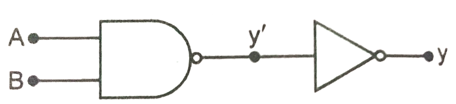
- The logic circuit Fig. represents
Text Solution
|
- Dicuss how the OR gate is realised from the NAND gate.
Text Solution
|
- The circuit in Fig.performs the logic function of
Text Solution
|
- In Boolean algbra barA.barB rquals
Text Solution
|
- The gate for which output is high, if atleast one input low is
Text Solution
|
- What will be the input of A and B for the Boolean expression bar((A+B)...
Text Solution
|
- The semiconductors available in narural form are called.............. ...
Text Solution
|
- The maximum possible energy possessed by free electrons of a material ...
Text Solution
|
- In energy band diagram, the energy gap for carbon (diamond)is....... .
Text Solution
|
- In.............semiconductor, the fermi level lies in the energy gap, ...
Text Solution
|
- In.............semiconductor, the fermi level lies in the energy gap, ...
Text Solution
|
- In n-type semocionductor, the..........are majority carries and..........
Text Solution
|
- In p-type semiconductors, the..........are majority carries and..........
Text Solution
|
- Those solids which have high conductivity and low resistivity are call...
Text Solution
|
- Those solids which have very low conductivity and very high resistivit...
Text Solution
|
- In p-n juction, the physical distance from one side of the barrier to ...
Text Solution
|
- A p-n junction can be considered to be equivalent to a..........with p...
Text Solution
|
- In p-n junction, p-side is known as........and n-side is known as........
Text Solution
|
- In germanium p-n diode, the ratio of reverse to forward resistance is....
Text Solution
|
- In p-n junction, there is a .................of majority carriers acro...
Text Solution
|