A
B
C
D
Text Solution
Verified by Experts
The correct Answer is:


Topper's Solved these Questions
Similar Questions
Explore conceptually related problems
CP SINGH-SEMICONDUCTORS-Exercises
- Pure Si at 500K has equal number of electron (n(e)) and hole (n(h)) co...
Text Solution
|
- A silicon specimen is made into a P-type semiconductor by dopping, on ...
Text Solution
|
- Which of the following energy band diagrams shows the N-type semicondu...
Text Solution
|
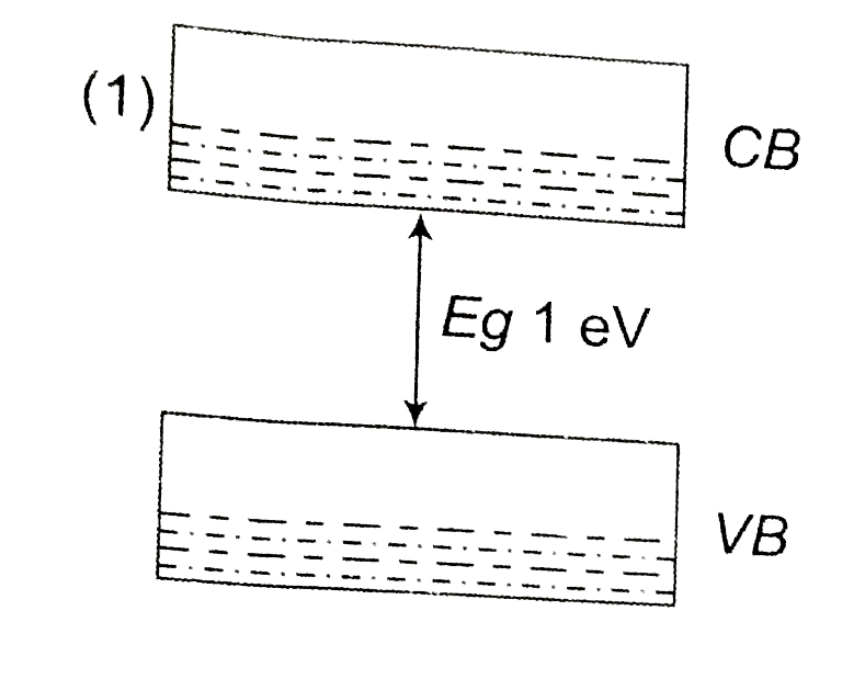
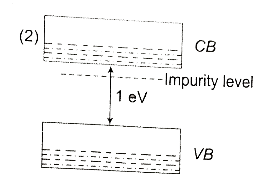
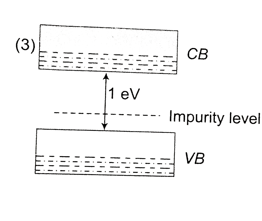
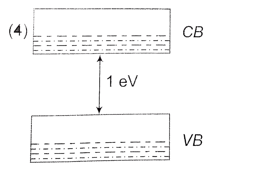
- The energy band diagrams for three semiconductor samples of silicon ar...
Text Solution
|
- In the energy band diagram of a material shown below, the open circles...
Text Solution
|
- The dominant mechanisms for motion of charge carriers in forward and r...
Text Solution
|
- A hole diffuses from the p-side to the n-side in a p-n junction.This m...
Text Solution
|
- In a p-n junction (i) new holes and conduction electrons are produce...
Text Solution
|
- In the case of forward biasing of PN-junction, which one of the follow...
Text Solution
|
- To make a PN junction conducting
Text Solution
|
- A potential barrier of 0.50 V exists across a P-N junction. If the de...
Text Solution
|
- The reverse biasing in a PN junction diode
Text Solution
|
- The cause of the potential barrier in a PN diode is
Text Solution
|
- The potential barrier, in the depletion layer, is due to
Text Solution
|
- Barrier potential of a p-n junction diode does not depend on
Text Solution
|
- The depletion layer in P-N junction region is caused by
Text Solution
|
- In a p- n junction diode not connected to any circuit,
Text Solution
|
- If the two ends of a p-n junction are joined by a wire ,
Text Solution
|
- A semiconducting device is connected in a series circuit with a batter...
Text Solution
|
- The PN junction diode is used as
Text Solution
|