Home
Class 12
PHYSICS
The energy band diagrams for three semic...

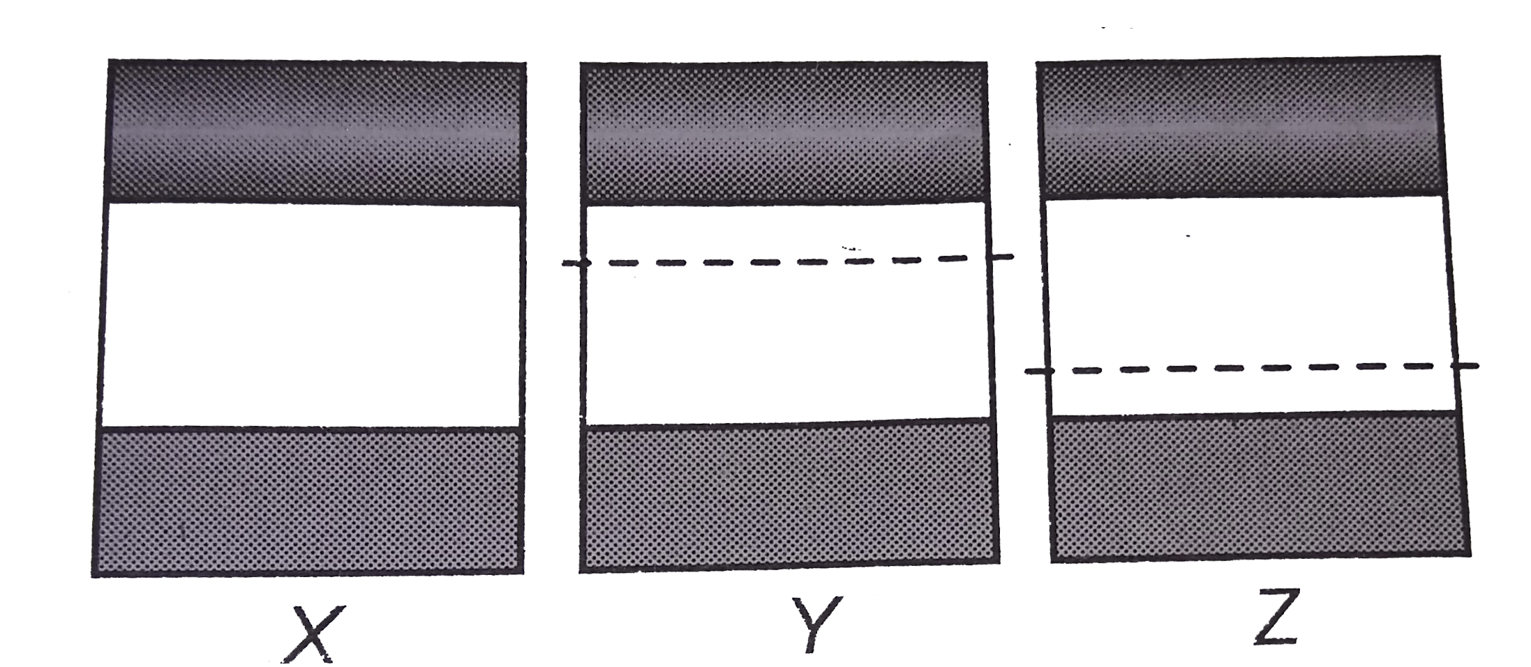
The energy band diagrams for three semiconductor samples of silicon are as shown. We can then assert that

A

Sample `X` is undoped while samples `Y` and `Z` have been doped with a third group and a fifth group impurity respectively

B

sample `X` is undoped while both samples `Y` and `Z` have been doped with a fifth grop impurity

C

sample `X` has been doped with equal amounts of third and fifth group impurities while samples `Y` and `Z` are undoped

D

sample `X` is undoped while samples `Y` and `Z` have been doped with a fifth group and a third impurity respectively

Text Solution

Verified by Experts

The correct Answer is:
D

NA
Promotional Banner

Topper's Solved these Questions

  • SEMICONDUCTORS

    CP SINGH|Exercise Exercises|140 Videos
  • REFRACTION OF LIGHT BY PLANE SURFACES

    CP SINGH|Exercise Exercises|110 Videos
  • THERMAL AND ELECTRIC EFFECT oF CURRENT

    CP SINGH|Exercise Exercises|101 Videos

Similar Questions

Explore conceptually related problems

From Energy Band Diagram

Draw the "energy bands" diagram for a (i) pure semiconductor (ii) insulator. How does the energy band, foe a pure semiconductor, get affected when this semiconductor is doped with an acceptor impurity donor impurity? Hence discuss why the 'holes' and the 'electrons' respectively, become the 'majority charge carriers' in these two cases.

Draw the energy band diagram of a p-type semiconductor. Deduce an expression for the conductivity of a p-type semiconductor.

Which of the following energy band diagrams shows the N -type semiconductor?

In energy band diagram, the energy gap for carbon (diamond)is....... .

CP SINGH-SEMICONDUCTORS-Exercises
  1. A silicon specimen is made into a P-type semiconductor by dopping, on ...

    Text Solution

    |

  2. Which of the following energy band diagrams shows the N-type semicondu...

    Text Solution

    |

  3. The energy band diagrams for three semiconductor samples of silicon ar...

    Text Solution

    |

  4. In the energy band diagram of a material shown below, the open circles...

    Text Solution

    |

  5. The dominant mechanisms for motion of charge carriers in forward and r...

    Text Solution

    |

  6. A hole diffuses from the p-side to the n-side in a p-n junction.This m...

    Text Solution

    |

  7. In a p-n junction (i) new holes and conduction electrons are produce...

    Text Solution

    |

  8. In the case of forward biasing of PN-junction, which one of the follow...

    Text Solution

    |

  9. To make a PN junction conducting

    Text Solution

    |

  10. A potential barrier of 0.50 V exists across a P-N junction. If the de...

    Text Solution

    |

  11. The reverse biasing in a PN junction diode

    Text Solution

    |

  12. The cause of the potential barrier in a PN diode is

    Text Solution

    |

  13. The potential barrier, in the depletion layer, is due to

    Text Solution

    |

  14. Barrier potential of a p-n junction diode does not depend on

    Text Solution

    |

  15. The depletion layer in P-N junction region is caused by

    Text Solution

    |

  16. In a p- n junction diode not connected to any circuit,

    Text Solution

    |

  17. If the two ends of a p-n junction are joined by a wire ,

    Text Solution

    |

  18. A semiconducting device is connected in a series circuit with a batter...

    Text Solution

    |

  19. The PN junction diode is used as

    Text Solution

    |

  20. Two PN-junction can be connected in series by three different methods ...

    Text Solution

    |