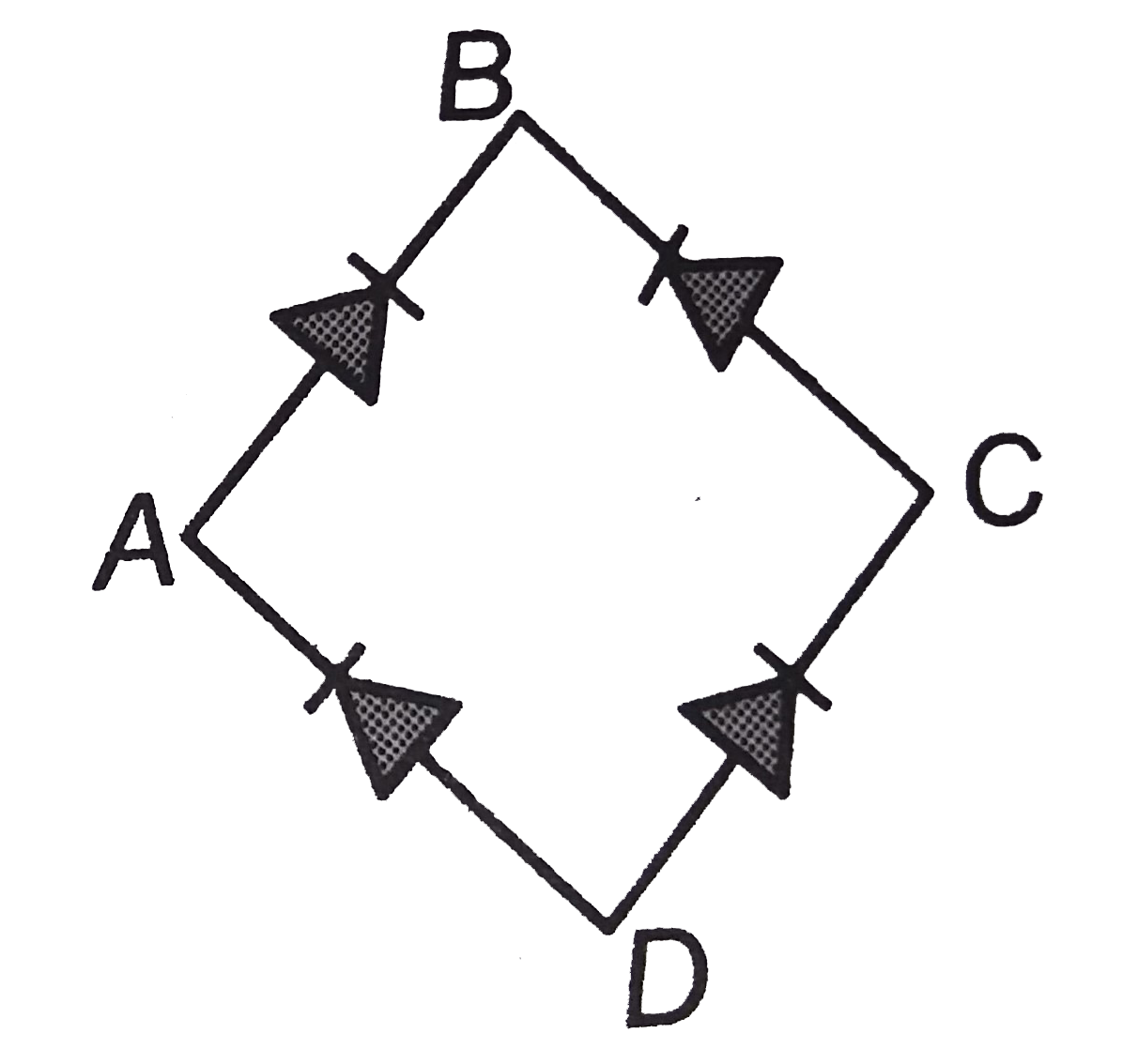
A
B
C
D
Text Solution
Verified by Experts
The correct Answer is:


Topper's Solved these Questions
Similar Questions
Explore conceptually related problems
CP SINGH-SEMICONDUCTORS-Exercises
- In the circuit given below, V(t) is the sinusiodal voltage source, vol...
Text Solution
|
- Which of the following is correct regarding bridge recifier?
Text Solution
|
- In the diagram, the input is across the terminals A and C and the outp...
Text Solution
|
- A bridge rectifier is shown in figure. Alternating input is given acro...
Text Solution
|
- In the circuit shown in figure the maximum output voltage V(0) is
Text Solution
|
- Which one of the following statement is not correct in the case of lig...
Text Solution
|
- A p-n photodiode is fabricate from a semiconductor with a band gap of ...
Text Solution
|
- A light emitting diode (LED) has a voltage drop of 2V across it and pa...
Text Solution
|
- GaAs (with a band gap =1.5eV) as an LED can emit
Text Solution
|
- Zener breakdown in a semi-conductor diode occurs when
Text Solution
|
- Zener breakdown takes place if
Text Solution
|
- Zener diode is used as
Text Solution
|
- A zener diode, having breakdown voltage equal to 15 V is used in a vol...
Text Solution
|
- If the voltage between the terminals A and B is 17V and zener breakdow...
Text Solution
|
- Least doped region in a transistor
Text Solution
|
- The part of a transistor which is most heavily doped to produce large ...
Text Solution
|
- If l(1),l(2),l(3) are the lengths of the emitter, base and collector o...
Text Solution
|
- The symbol given in figure represents
Text Solution
|
- In a transistor base is made thin and doped with little impurity atoms...
Text Solution
|
- In a normal operation of a transistor, (i) base-emitter junction is ...
Text Solution
|