A
B
C
D
Text Solution
Verified by Experts
The correct Answer is:


Topper's Solved these Questions
Similar Questions
Explore conceptually related problems
RESONANCE-SEMICONDUCTORS-Exercise 3
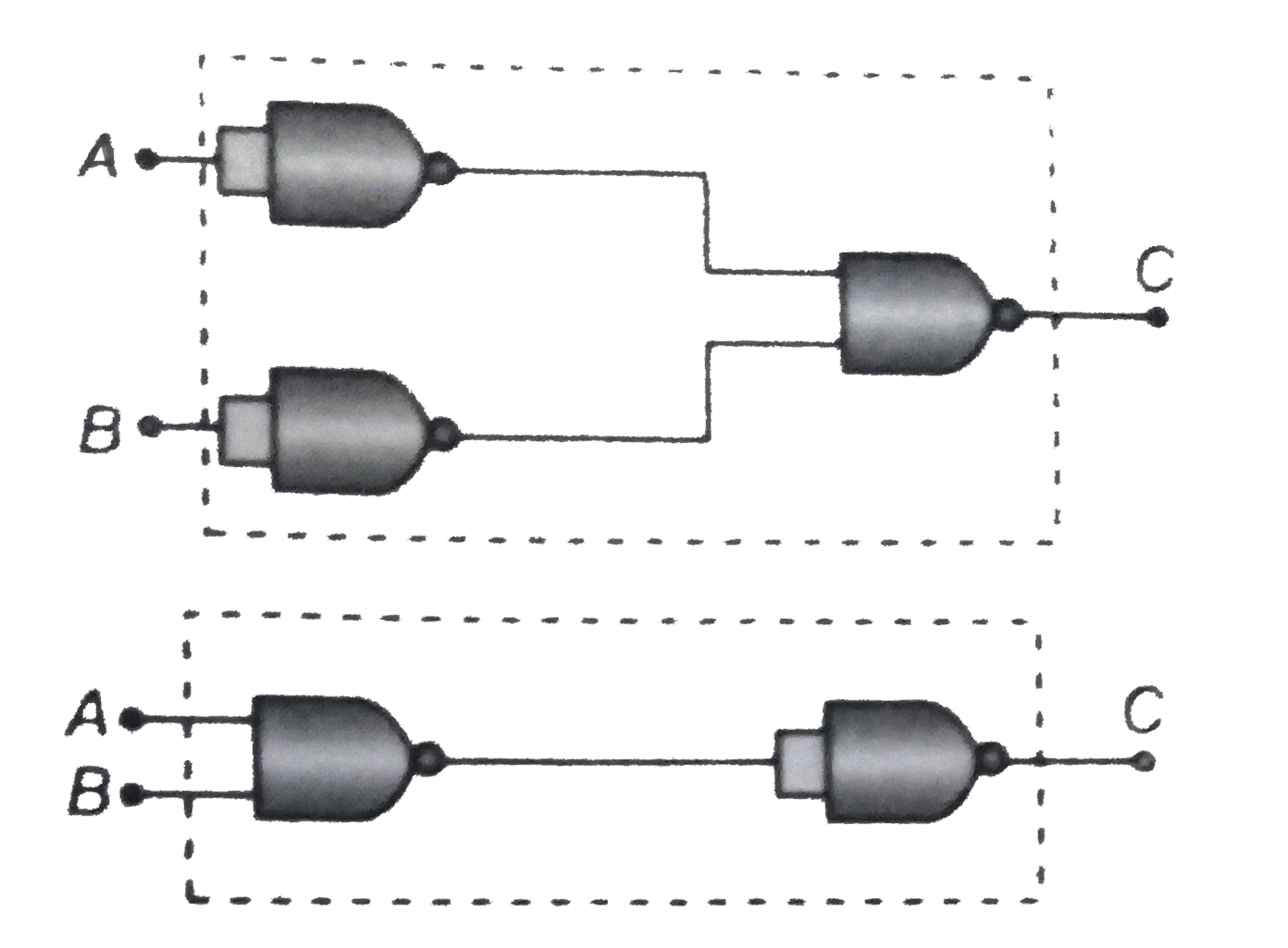
- The combination of 'NAND' gates shown here under (figure) are equivale...
Text Solution
|
- When p-n junction diode is forward biased then
Text Solution
|
- When npn transistor is used as an amplifler
Text Solution
|
- The electrical conductivity of a semiconductor increases when electrom...
Text Solution
|
- In a common base ampifier , the phase difference between the input sig...
Text Solution
|
- If a full wave reactifier circuit is operating from 50 Hz mains, the f...
Text Solution
|
- If the ratio of the concentration of electron to that of holes in a se...
Text Solution
|
- In a common base mode of a transition , the collector current is 5.48...
Text Solution
|
- If the lattice constant of this semiconductor is decreased, then which...
Text Solution
|
- The circuit has two oppositively connected ideal diodes in parallel wh...
Text Solution
|
- If a p-n junction diode, a square input signal of 10 V is applied as s...
Text Solution
|
- Carbon , silicon and germanium have four valence electrons each . At r...
Text Solution
|
- A working transitor with its three legs marked P, Q and R is tested us...
Text Solution
|
- In the circuit below, A and B represents two inputs and C represents t...
Text Solution
|
- The Fig shown input waveforms A and B to a logic gate. Draw the output...
Text Solution
|
- a p -n juction (D) shown in the figure can act an a rectifier An alter...
Text Solution
|
- The output of an OR gate is connected to both the inputs of a NAND gat...
Text Solution
|
- Truth table for system of four NAND gates as shown in figure is : .
Text Solution
|
- The 1- V characteristic of on LED is
Text Solution
|
- The forward biased diode connection is
Text Solution
|
- Two identical p-n junctions may be connected in series in which a batt...
Text Solution
|