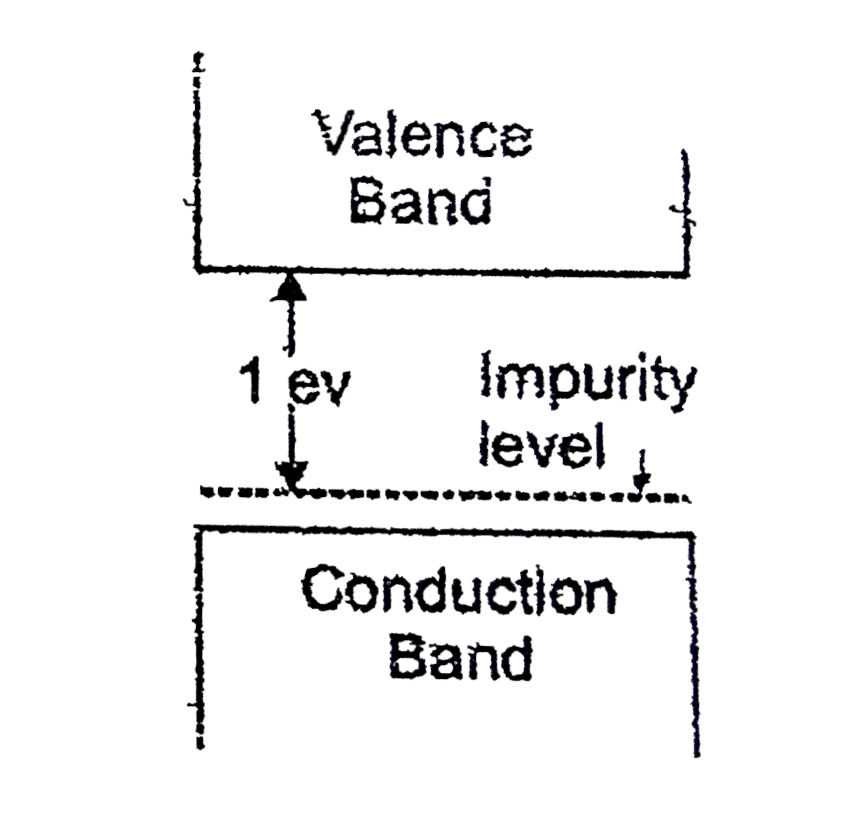
A
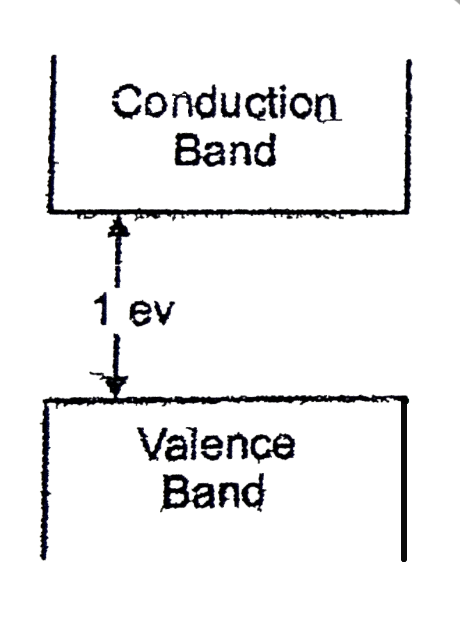
B
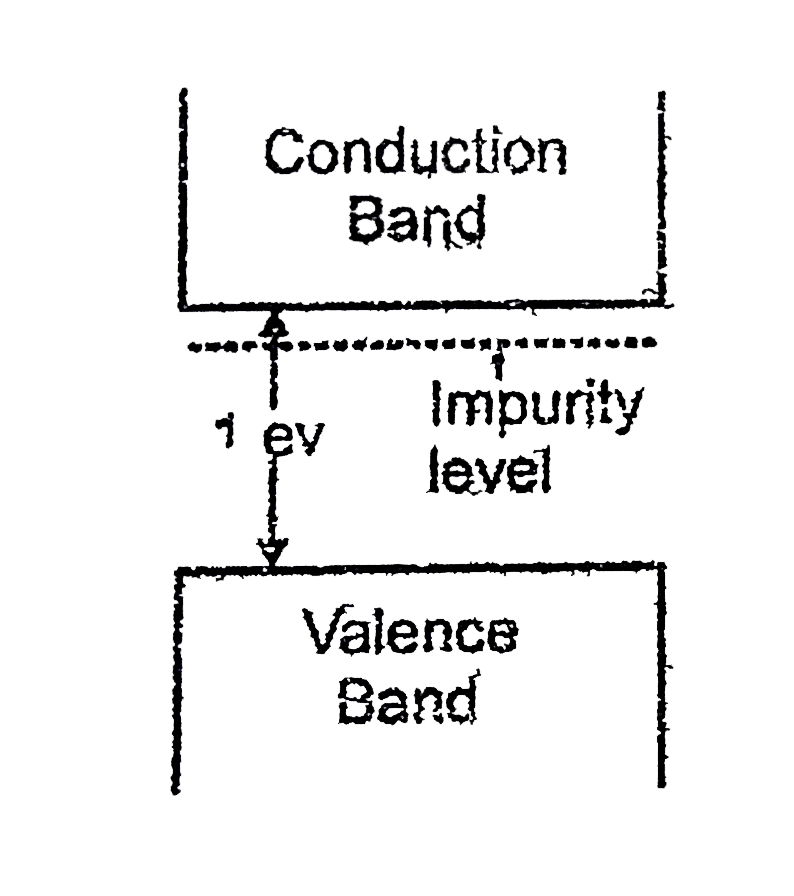
C
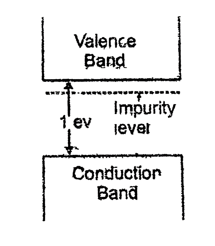
D
Text Solution
Verified by Experts
The correct Answer is:


Topper's Solved these Questions
Similar Questions
Explore conceptually related problems
RESONANCE-SEMICONDUCTORS-Exercise
- A semiconductor is doped with a donor impurity
Text Solution
|
- A P-type semiconductor has acceptor levels 57 meV above the valence ba...
Text Solution
|
- Which of the following energy band diagrams shows the N-type semicondu...
Text Solution
|
- A P-type sillicon semiconductor is made by adding one atom of indium p...
Text Solution
|
- When N-type of semiconductor is heated
Text Solution
|
- GaAs is-
Text Solution
|
- What will be conductance of pure sillicon crystal at 300 K temp? if el...
Text Solution
|
- Forbidden energy gap of Ge is 0.75eV, maximum wave length of incident ...
Text Solution
|
- Mobility of electron in N-type Ge is 5000 cm^(2)//"volt" sec and condu...
Text Solution
|
- The intrinsic carrier density in germanium crystal at 300 K is 2.5xx10...
Text Solution
|
- Pure Si at 300 K has equal electron (n(e)) and hole (n(h)) concentrati...
Text Solution
|
- The length of a germanium rod is 0.58 cm and its area of cross-section...
Text Solution
|
- The contribution in the total current flowing through a semiconductor ...
Text Solution
|
- The P-N junction is-
Text Solution
|
- Diffusion current in a p-n junction is greater than the drift current ...
Text Solution
|
- In a p-n junction
Text Solution
|
- A hole diffuses from the p-side to the n-side in a p-n junction.This m...
Text Solution
|
- The depletion region of a P-N diode, under open circuit condition cont...
Text Solution
|
- Which is the wrong statement in following sentence? A device in which ...
Text Solution
|
- The depletion layer in P-N junction region is caused by
Text Solution
|