 .
.A
B
C
D
Text Solution
Verified by Experts
The correct Answer is:


Topper's Solved these Questions
Similar Questions
Explore conceptually related problems
RESONANCE-SEMICONDUCTORS-Exercise 3
- If the lattice constant of this semiconductor is decreased, then which...
Text Solution
|
- The circuit has two oppositively connected ideal diodes in parallel wh...
Text Solution
|
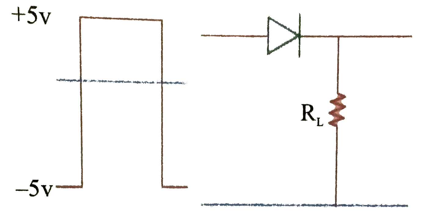
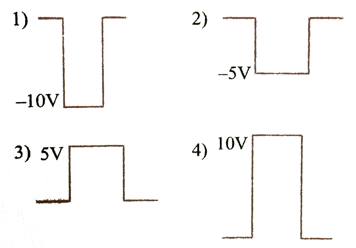
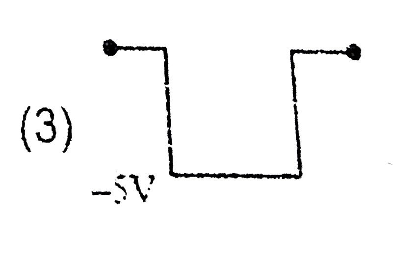
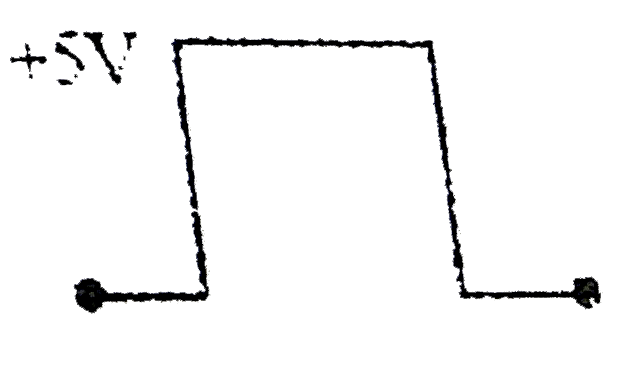
- If a p-n junction diode, a square input signal of 10 V is applied as s...
Text Solution
|
- Carbon , silicon and germanium have four valence electrons each . At r...
Text Solution
|
- A working transitor with its three legs marked P, Q and R is tested us...
Text Solution
|
- In the circuit below, A and B represents two inputs and C represents t...
Text Solution
|
- The Fig shown input waveforms A and B to a logic gate. Draw the output...
Text Solution
|
- a p -n juction (D) shown in the figure can act an a rectifier An alter...
Text Solution
|
- The output of an OR gate is connected to both the inputs of a NAND gat...
Text Solution
|
- Truth table for system of four NAND gates as shown in figure is : .
Text Solution
|
- The 1- V characteristic of on LED is
Text Solution
|
- The forward biased diode connection is
Text Solution
|
- Two identical p-n junctions may be connected in series in which a batt...
Text Solution
|
- In a p- n junction diode not connected to any circuit,
Text Solution
|
- For the given circult shown in fig to act as full wave rectifer , the ...
Text Solution
|
- In a....... baised pn junction , the net flow of holes is from the n ...
Text Solution
|
- The cause of the potential barrier in a p-n diode is:
Text Solution
|
- The transfer ration of a transistor is 50. The input resistance of th...
Text Solution
|
- When added an impurity into the silicon which one of the following pro...
Text Solution
|
- In junction diode, the holes are due to
Text Solution
|