A
B
C
D
Text Solution
Verified by Experts


Topper's Solved these Questions
Similar Questions
Explore conceptually related problems
DISHA-SEMICONDUCTOR-physics
- For a transistor (I(C))/(I(E))=0.96, then current gain for common emit...
Text Solution
|
- Given below are symbols for some logic gates :- The XOR gate and ...
Text Solution
|
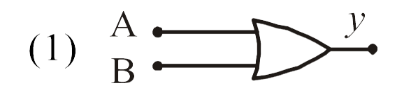
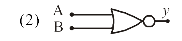
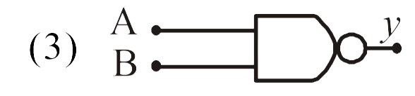
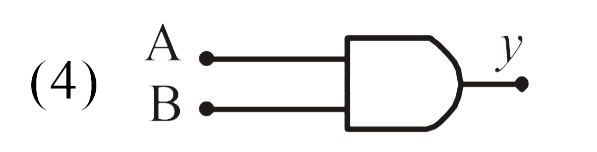
- Given below are four logic gates symbol (figure). Those for OR, NOR an...
Text Solution
|
- Assertion: The logic gate NOT can be built using diode. Reason: The ...
Text Solution
|
- Assertion: The following circuit represents 'OR' gate Reason: For...
Text Solution
|
- Assertion: De Morgan's theoram bar(A+B)=bar(A).bar(B) may be explained...
Text Solution
|
- When a semiconductor is heated, its resistance
Text Solution
|
- The energy band gap of Si is
Text Solution
|
- The forbidden energy band gap in conductors, semiconductors and insula...
Text Solution
|
- Let n(p) and n(e) be the number of holes and conduction electrons resp...
Text Solution
|
- Which statement is correct?
Text Solution
|
- Wires P and Q have the same resistance at ordinary (room) temperature....
Text Solution
|
- In extrinsic P and N - type, semiconductor materials, the ratio of the...
Text Solution
|
- At zero Kelvin a piece of germanium
Text Solution
|
- Electronical configuration of germenium is 2,8,18 and 4. To make it ex...
Text Solution
|
- The intrinsic semiconductor becomes an insulator at
Text Solution
|
- Energy band in solids are a consequence of
Text Solution
|
- In energy band diagram, the energy gap for carbon (diamond)is....... .
Text Solution
|
- The valence band and conduction band of a solid overlap at low temper...
Text Solution
|
- Choose the correct statement
Text Solution
|