A
B
C
D
Text Solution
Verified by Experts


Topper's Solved these Questions
Similar Questions
Explore conceptually related problems
DISHA-SEMICONDUCTOR-PHYSICS
- In an n-p-n transistor 10^(10) electrons enter the emitter in 10^(-6)s...
Text Solution
|
- Assuming that the silicon diode having resistance of 20 Omega, the cur...
Text Solution
|
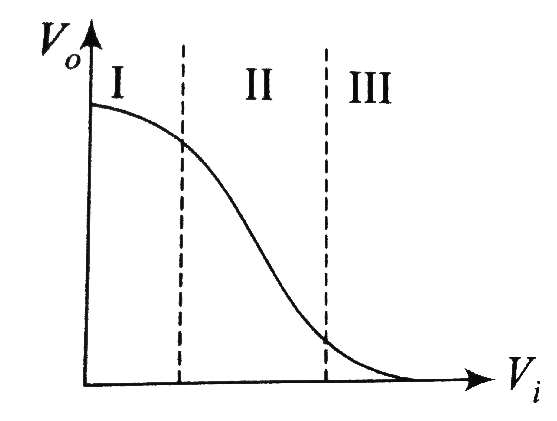
- Transfer characterstics [output voltage (V(o)) vs. input voltage (V(i)...
Text Solution
|
- A half-wave rectifier is being used to rectify an alternating voltage ...
Text Solution
|
- A diode having potential difference 0.5 V across its junction which do...
Text Solution
|
- In common emitter amplifier, the current gain is 62. The collector res...
Text Solution
|
- On doping germanium with donor atoms of density 10^(17) cm^(-3), find ...
Text Solution
|
- The voltage gain of an amplifier with 9% negative feedback is 10. The ...
Text Solution
|
- A system of four gates is set up as shown. The 'truth table' correspon...
Text Solution
|
- The intrinsic conductivity of germanium at 27^(@) is 2.13 mho m^(-1) a...
Text Solution
|
- The logic circuit shown below has the input waveforms ‘A’ and ‘B’ as s...
Text Solution
|
- Pure Si at 500K has equal number of electron (n(e)) and hole (n(h)) co...
Text Solution
|
- Which of the following statements is incorrect?
Text Solution
|
- The relation between number of free electrons (n) in a semiconductor a...
Text Solution
|
- If a PN junction diode of depletion layer width W and barrier height V...
Text Solution
|
- The circuit has two oppositively connected ideal diodes in parallel wh...
Text Solution
|
- For a transistor ampliflier in common emiter configuration for load im...
Text Solution
|
- A PN - junction has a thickness of the order of
Text Solution
|
- A working transitor with its three legs marked P, Q and R is tested us...
Text Solution
|
- If a p-n junction diode, a square input signal of 10 V is applied as s...
Text Solution
|