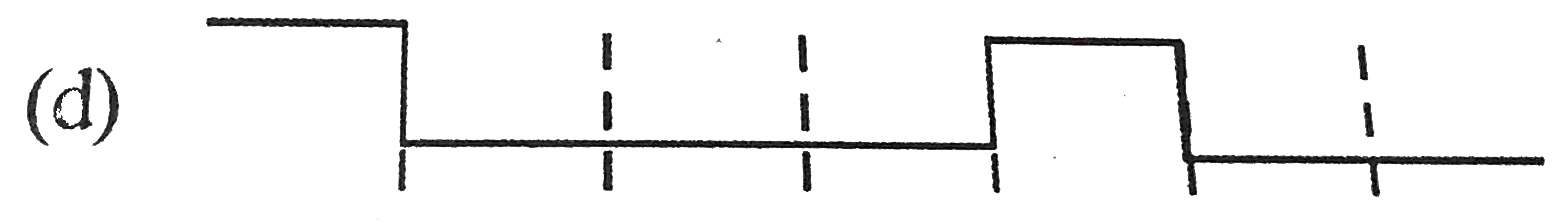
A
B
C
D
Text Solution
Verified by Experts


Topper's Solved these Questions
Similar Questions
Explore conceptually related problems
DISHA-SEMICONDUCTOR-PHYSICS
- A system of four gates is set up as shown. The 'truth table' correspon...
Text Solution
|
- The intrinsic conductivity of germanium at 27^(@) is 2.13 mho m^(-1) a...
Text Solution
|
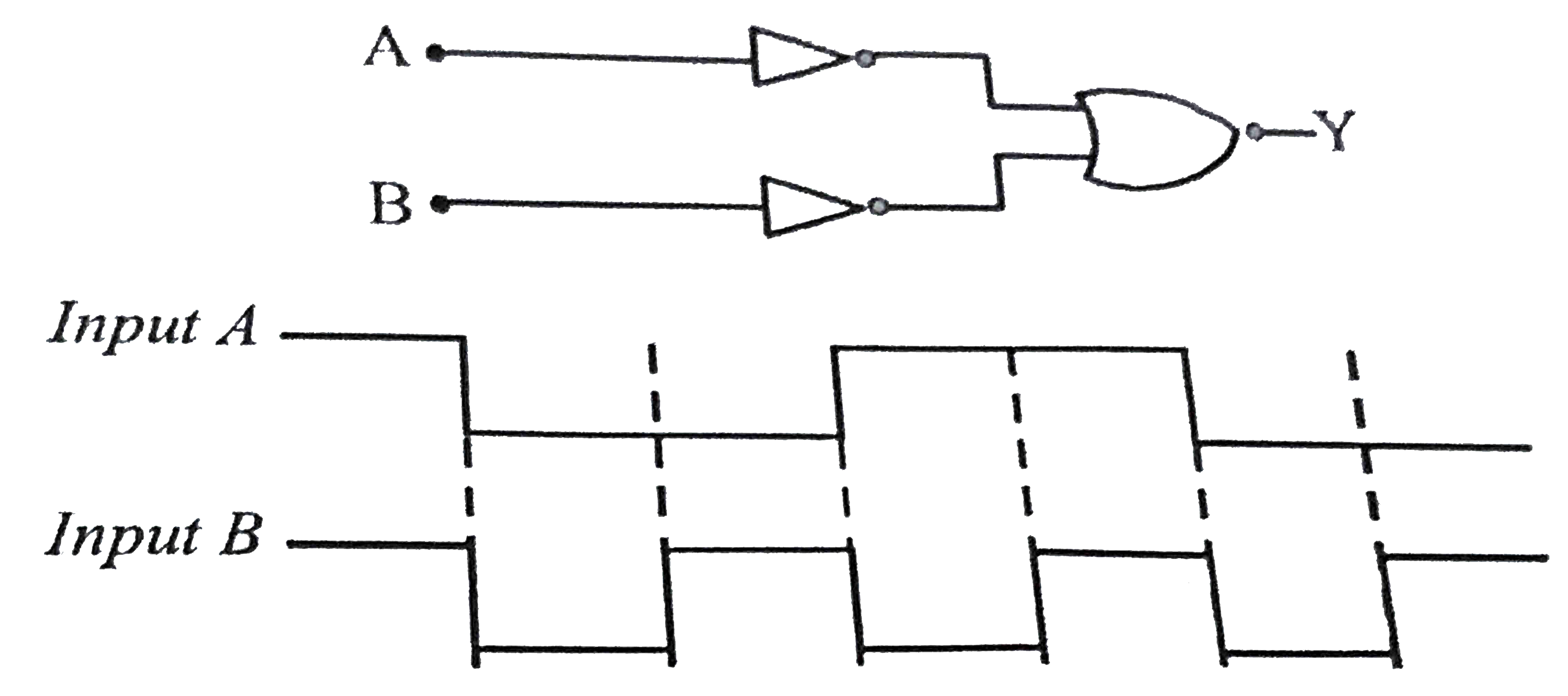
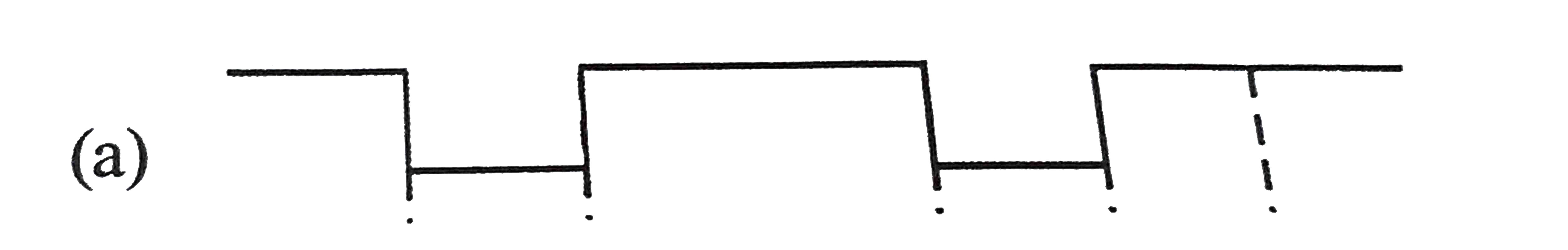
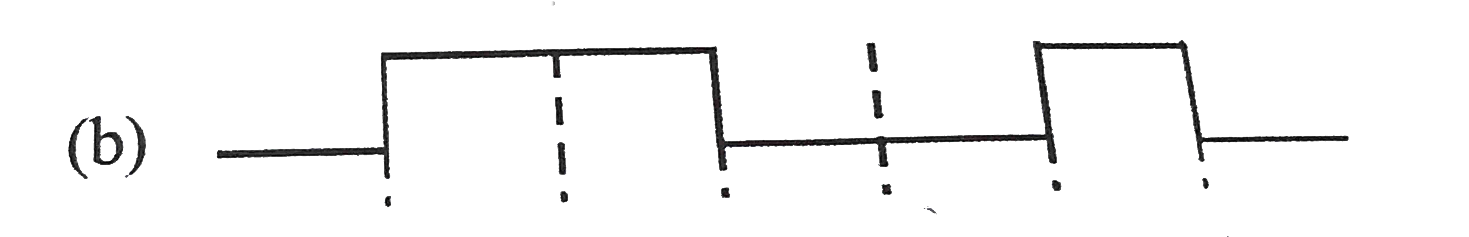
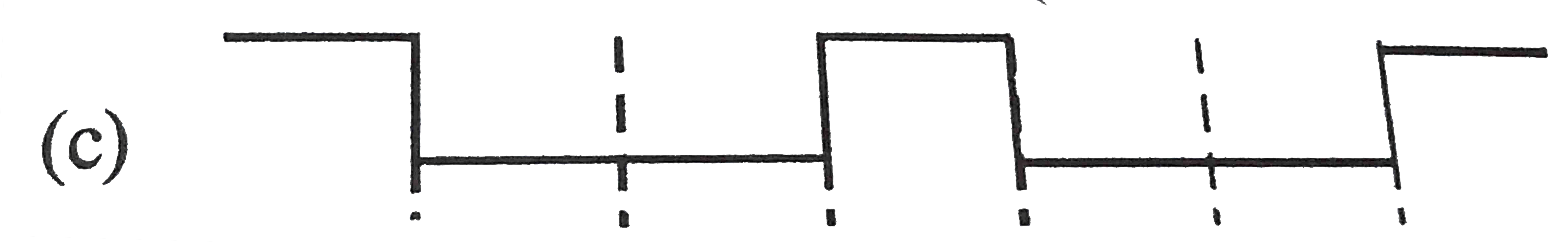
- The logic circuit shown below has the input waveforms ‘A’ and ‘B’ as s...
Text Solution
|
- Pure Si at 500K has equal number of electron (n(e)) and hole (n(h)) co...
Text Solution
|
- Which of the following statements is incorrect?
Text Solution
|
- The relation between number of free electrons (n) in a semiconductor a...
Text Solution
|
- If a PN junction diode of depletion layer width W and barrier height V...
Text Solution
|
- The circuit has two oppositively connected ideal diodes in parallel wh...
Text Solution
|
- For a transistor ampliflier in common emiter configuration for load im...
Text Solution
|
- A PN - junction has a thickness of the order of
Text Solution
|
- A working transitor with its three legs marked P, Q and R is tested us...
Text Solution
|
- If a p-n junction diode, a square input signal of 10 V is applied as s...
Text Solution
|
- When N-type of semiconductor is heated
Text Solution
|
- The ratio of electron and hole currents in a semiconductor is 7/4 and ...
Text Solution
|
- C and Si both have same lattice structure, having 4 bonding electrons ...
Text Solution
|
- Which one of the following represents forward bias diode?
Text Solution
|
- An oscillator is nothing but an amplifier with
Text Solution
|
- The current gain in the common emitter mode of a transistor is 10. The...
Text Solution
|
- The input signal given to a CE amplifier having a voltage gain of 150 ...
Text Solution
|
- In the use of transistor as an amplifier
Text Solution
|