 .
.A
B
C
D
Text Solution
Verified by Experts
The correct Answer is:


Topper's Solved these Questions
Similar Questions
Explore conceptually related problems
BANSAL-MASTER PRACTICE PROBLEM-Additional topic
- The logic circuit shown below has the input waveforms ‘A’ and ‘B’ as s...
Text Solution
|
- The combination of gates shown below yields .
Text Solution
|
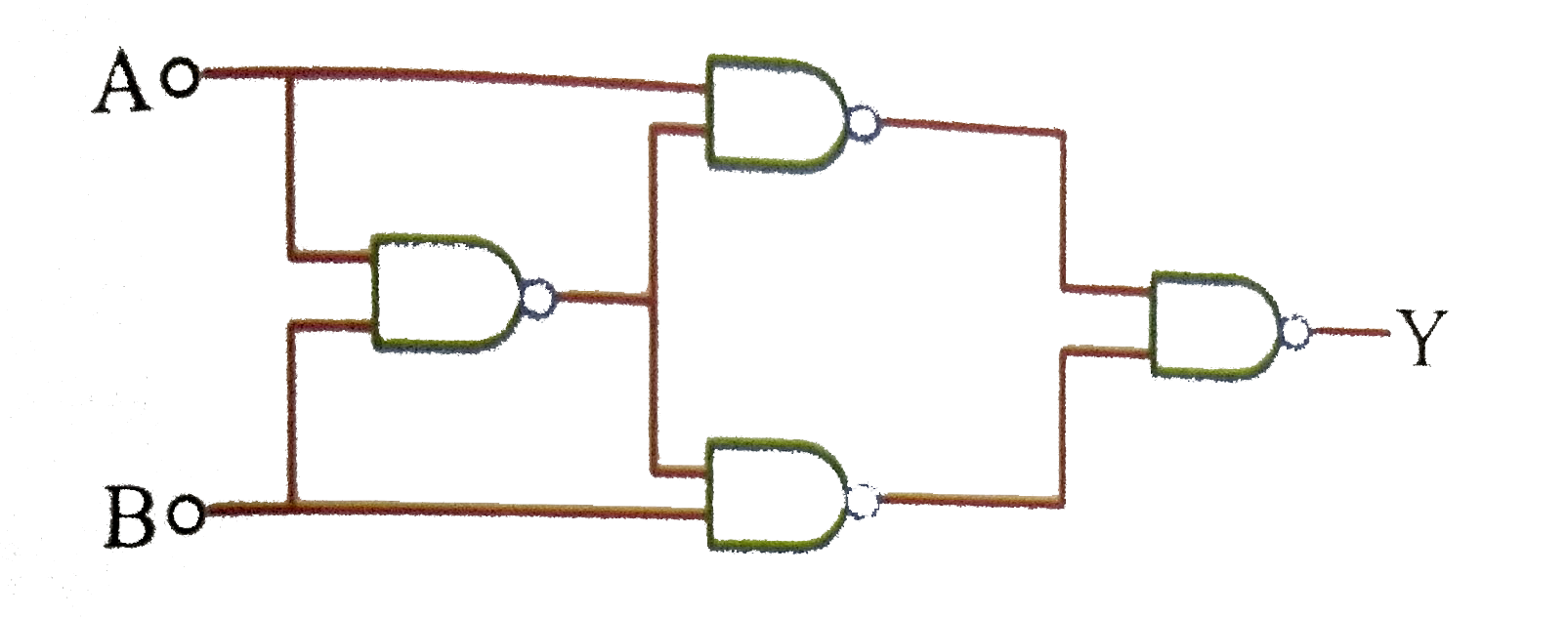
- Truth table for system of four NAND gates as shown in figure is : .
Text Solution
|
- In semiconductor the concentrations of electron and holes are 8xx10^(1...
Text Solution
|
- A potential difference of 2V is applied between the opposite faces of ...
Text Solution
|
- The main cause of avalence breakdown is
Text Solution
|
- A cube of germanium is placed between the poles of a magnet and a volt...
Text Solution
|
- In the given figure, which of the diodes are forward biased?
Text Solution
|
- Current in the circuit will be
Text Solution
|
- The diode used in the circuit shown in the figure has a constant volta...
Text Solution
|
- In the following circuits PN-junction diodes D(1), D(2) and D(3) are i...
Text Solution
|
- A sinusoidal voltage of peak value 200 volts is connected to a diode a...
Text Solution
|
- In the figure an A.C of rms voltage 200 volt is appled to the circuit ...
Text Solution
|
- In the circuit shown in figure, Voltage V(0) is
Text Solution
|
- In the given circuit V(O(1))&V(O(2)) are
Text Solution
|
- Which is the correct diagram of a half- wave reactifier?
Text Solution
|
- In the diagram, the input is across the terminals A and C and the outp...
Text Solution
|
- A full wave rectifier circuit along with the input and output are show...
Text Solution
|
- An NPN-transistor circuit is arranged as shown in figure. It is
Text Solution
|
- Given below are four logic gates symbol (figure). Those for OR, NOR an...
Text Solution
|