A
B
C
D
Text Solution
Verified by Experts
The correct Answer is:


Topper's Solved these Questions
Similar Questions
Explore conceptually related problems
BANSAL-MASTER PRACTICE PROBLEM-Additional topic
- A sinusoidal voltage of peak value 200 volts is connected to a diode a...
Text Solution
|
- In the figure an A.C of rms voltage 200 volt is appled to the circuit ...
Text Solution
|
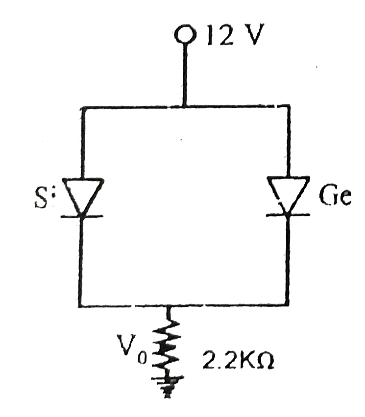
- In the circuit shown in figure, Voltage V(0) is
Text Solution
|
- In the given circuit V(O(1))&V(O(2)) are
Text Solution
|
- Which is the correct diagram of a half- wave reactifier?
Text Solution
|
- In the diagram, the input is across the terminals A and C and the outp...
Text Solution
|
- A full wave rectifier circuit along with the input and output are show...
Text Solution
|
- An NPN-transistor circuit is arranged as shown in figure. It is
Text Solution
|
- Given below are four logic gates symbol (figure). Those for OR, NOR an...
Text Solution
|
- Which of the following gates will have an output of 1
Text Solution
|
- The combination of 'NAND' gates shown here under (figure) are equivale...
Text Solution
|
- For the given combination of gates, if the logic states of inputs A,B,...
Text Solution
|
- Which logic gate is represented by the following combination of logic ...
Text Solution
|
- A. The energy band of valence electrons is called Valence band B. The ...
Text Solution
|
- A Both Valance band and conduction band can accommodate equal number o...
Text Solution
|
- A. it is impossible to get a completely filled conduction band. B. It ...
Text Solution
|
- A.A diode merely converts A.C. into D.C.B.A diode cannot given amplifi...
Text Solution
|
- Statement 1: Conductivity of semiconductor increases with increase in ...
Text Solution
|
- Statement 1: Conductivity of semiconductors decreases with increase in...
Text Solution
|
- Statement 1: In semiconductors current is obtained due to motion of el...
Text Solution
|