Home
Class 12
PHYSICS
In the junction transistor voltage ampli...


In the junction transistor voltage amplifier circuit of figure, if `R_(1)=100kOmega,R_(2)=1kOmega,V_(C C)=6.0V` and `V_(BE)=0.6V` current gain=60

A

`I_(B)=54muA`

B

`I_(C)=3.24mA`

C

the voltage across `R_(2)=3.24V`

D

the voltage across the collector-emitter=3.24V

Text Solution

Verified by Experts

The correct Answer is:
A, B, C
Promotional Banner

Topper's Solved these Questions

  • SEMICONDUCTORS

    BANSAL|Exercise Exercise-3|24 Videos
  • SEMICONDUCTORS

    BANSAL|Exercise Exercise-4|37 Videos
  • SEMICONDUCTORS

    BANSAL|Exercise CBSE Question|32 Videos
  • MASTER PRACTICE PROBLEM

    BANSAL|Exercise Additional topic|70 Videos
  • TEST PAPERS

    BANSAL|Exercise PHYSICS PART C|14 Videos

Similar Questions

Explore conceptually related problems

In a transistor connected in a common emitter mode it has, R_(c)=4kOmega, R_(i)=1kOmega, I_(c)=1mA and I_(b)= 20 muA. Find the voltage gain.

In a transistor, connected in common emitter mode R_(0)=5kOmega," "R_(i)=1kOmega," "I_(C)=1mA,I_(B)=40muA . Find the voltage gain.

In a transistor connected in a common emitter mode R_C = 4kOmega, R_1 = 1kOmega, I_C = 1mA and I_B = 20 muA . Find the voltage gain.

Passage I An n-p-n transistor is used as a voltage amplifier in a commoin emitter circuit given V_(CC)=8V I_(C )=4mA V_(CE)=4V, (V_(BE)=0.6 V, V_(BB)=8V beta_(Dc)=200 The value of load resistqacne is

In common emitter transistor as shown in Fig., the V_(BB) supply can be varied from 0 V to 5.0V. The Si. Transistor has beta_(ac)=250 and R_(B)=100kOmega, R_(c)=1k Omega,V_(C C)=5.0V . Assume that when the transistor is saturated, V_(CE)=0V and V_(BE)=0.8V . Calculate the minimum base current, for which the transistor will reach saturation. Hance, determine V_(i) when the transistor is 'switched on' find ranges of V_(i) for which the transistor is switched off and switched on.

In the circuit shown below E_(1) = 4.0 V, R_(1) = 2 Omega, E_(2) = 6.0 V, R_(2) = 4 Omega and R_(3) = 2 Omega . The current I_(1) is

A common emitted amplifier circuit, built using an npn transistor, is shown in the figure. Its dc current gain is 250,R_(C)=1Komega and V_(C C)=10V . What is the minimum base current for V_(CE) to reach saturation?

In the figure shown , R_B=500kOmega, R_C = 8 kOmega, V_("BB")=10.6V and V_("CC") = 20V . The current amplification factor beta=100 and V_("BE")=0.6 V . Mark the incorrect statement .

BANSAL-SEMICONDUCTORS-Exercise-2
  1. Statement-1 surface wave and sky wave can not be observed on moon. S...

    Text Solution

    |

  2. Statement 1: In ground wave transmission the radio signals die out aft...

    Text Solution

    |

  3. Statement 1: Ground wave communication is effective only at low freque...

    Text Solution

    |

  4. Statement 1: The refractive index of the ionosphere increases as we go...

    Text Solution

    |

  5. Statement 1: Sky wave communication is not suitable for frequencies gr...

    Text Solution

    |

  6. Statement 1: Microwaves and not radiowaves are used in satellite commu...

    Text Solution

    |

  7. Statement 1: Long distance radio broadcasts use short wave bands. St...

    Text Solution

    |

  8. Statement 1: Sky wave communication is not used to transmit TV signals...

    Text Solution

    |

  9. The question has statement - 1 and statement - 2 Of the four choices ...

    Text Solution

    |

  10. The physical property (ies) which (is) are same along all the directio...

    Text Solution

    |

  11. Choose the wrong statement

    Text Solution

    |

  12. Which of the following statements is correct-

    Text Solution

    |

  13. The materials resistance of which decreases with increases in temperat...

    Text Solution

    |

  14. Which of the following statements is correct-

    Text Solution

    |

  15. Pick the correct statement the reverse current in p-n junction diode

    Text Solution

    |

  16. In a p-n junction–

    Text Solution

    |

  17. Two identical p-n junctions may be connected in series in which a batt...

    Text Solution

    |

  18. For the circuit shown in the figure:

    Text Solution

    |

  19. The avalanche break down in p-n junction is not caused due to

    Text Solution

    |

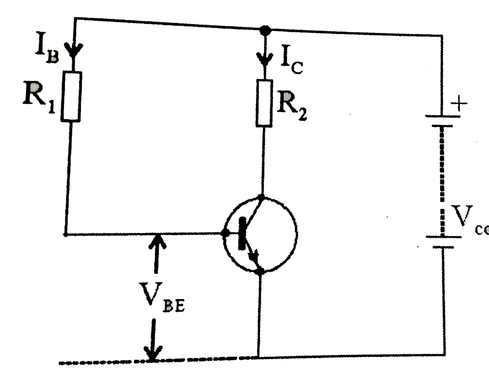
  20. In the junction transistor voltage amplifier circuit of figure, if R(1...

    Text Solution

    |