


Topper's Solved these Questions
Similar Questions
Explore conceptually related problems
BANSAL-SEMICONDUCTORS-CBSE Question
- How does the width of the depletion layer of a p-n junction diode chan...
Text Solution
|
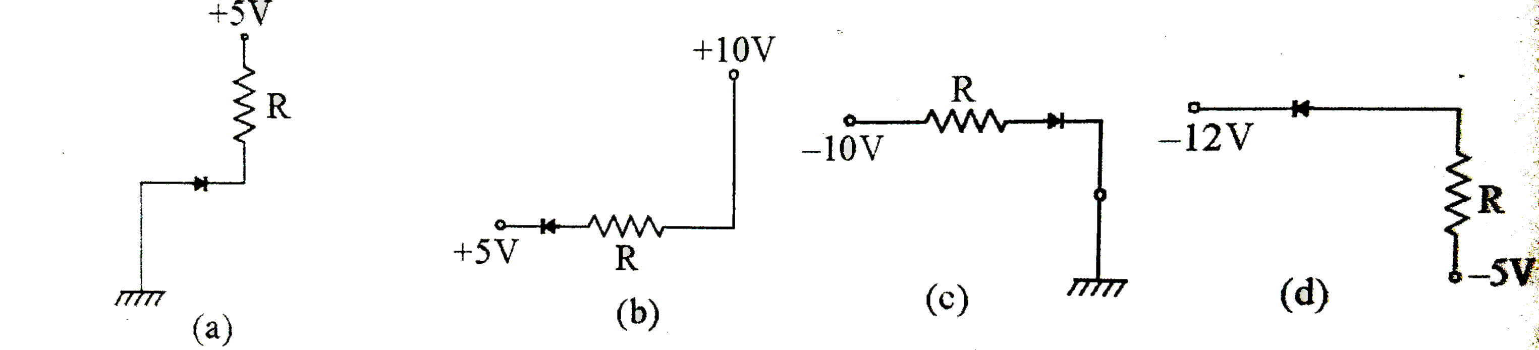
- In the following diagrams, write which of the nodes are forward biased...
Text Solution
|
- The output of a 2-inputs NAND gate is fed to a NOT gate. Write down th...
Text Solution
|
- ZENER DIODE AS VOLTAGE REGULATOR
Text Solution
|
- Draw a labelled circuit diagram for a common emitter amplifier using n...
Text Solution
|
- Name of gate obtained from the combination of gates shown in the figur...
Text Solution
|
- How is p-type semiconductor formed? Name the major charge carriers in ...
Text Solution
|
- ZENER DIODE AS VOLTAGE REGULATOR
Text Solution
|
- Draw a labelled circuit diagram of a common base amplifier using a p-n...
Text Solution
|
- Draw the voltage current characteristic fo a zener diode.
Text Solution
|
- With the help of a labelled circuit diagram, explain how an n-p-n tran...
Text Solution
|
- Give the logic symbol for an OR gate. Draw the output wave form for in...
Text Solution
|
- How does the resistivity of (i) a conductor and (ii) a semiconductor v...
Text Solution
|
- Distinguish between conductor (or metals), semiconductors and insulato...
Text Solution
|
- (a). Explains briefly with the help of a circuit diagram how V-I chara...
Text Solution
|
- Explain (i) forward biasing (ii) reverse biasing of a P-N junction dio...
Text Solution
|
- Distinguish between conductor (or metals), semiconductors and insulato...
Text Solution
|
- Two semiconductor materials X and Y shown in the given figure, are mad...
Text Solution
|
- Draw the circuit diagram of a common emitter amplifier using n-p-n tra...
Text Solution
|
- Expalin the formation of energy band in solids. Draw energy band diagr...
Text Solution
|