


BANSAL-SEMICONDUCTORS-CBSE Question
- How does the resistivity of (i) a conductor and (ii) a semiconductor v...
Text Solution
|
- Distinguish between conductor (or metals), semiconductors and insulato...
Text Solution
|
- (a). Explains briefly with the help of a circuit diagram how V-I chara...
Text Solution
|
- Explain (i) forward biasing (ii) reverse biasing of a P-N junction dio...
Text Solution
|
- Distinguish between conductor (or metals), semiconductors and insulato...
Text Solution
|
- Two semiconductor materials X and Y shown in the given figure, are mad...
Text Solution
|
- Draw the circuit diagram of a common emitter amplifier using n-p-n tra...
Text Solution
|
- Expalin the formation of energy band in solids. Draw energy band diagr...
Text Solution
|
- Distinguish between intrinsic semiconductor and p-type semiconductor. ...
Text Solution
|
- The give inputs A, B are fed to a 2-input NAND gate. Draw the output w...
Text Solution
|
- The output of a 2-input AND gate is fed to a NOT gate. Give the name o...
Text Solution
|
- Draw a circuit diagram of a transistor amplifier in CE configuration. ...
Text Solution
|
- Explain (i) forward biasing (ii) reverse biasing of a P-N junction dio...
Text Solution
|
- In V-I characteristics of a p-n junction diode, why is the current und...
Text Solution
|
- (i) Identify the logic gates marked P and Q in the given logic circuit...
Text Solution
|
- What happens to the width of depletion layer of a p-n junction when it...
Text Solution
|
- Draw a circuit diagram of a full-wave rectifier. Explain its working p...
Text Solution
|
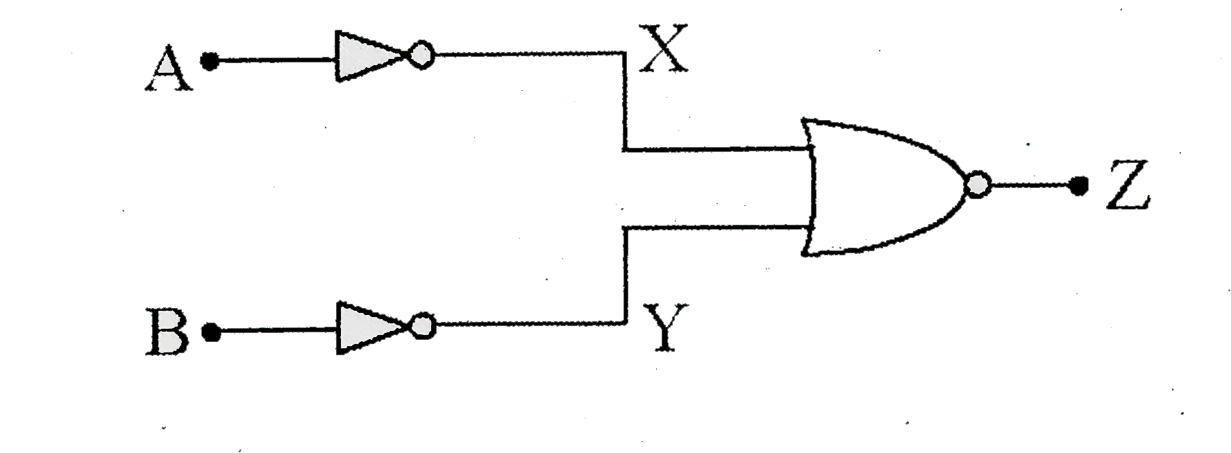
- You are given a circuit below. Write its truth table. Hence, identify ...
Text Solution
|
- Explain the formation of depletion layer and potential barrier in p-n ...
Text Solution
|
- Draw a circuit diagram of a full-wave rectifier. Explain its working p...
Text Solution
|