A
B
C
D
Text Solution
Verified by Experts
The correct Answer is:


Topper's Solved these Questions
Similar Questions
Explore conceptually related problems
NEET PREVIOUS YEAR (YEARWISE + CHAPTERWISE)-SOLID AND SEMICONDUCTOR DEVICES-Exercise
- The device that can act as a complete electronic circuit is
Text Solution
|
- A common emitter amplifier has a voltage gain of 50, an input impedenc...
Text Solution
|
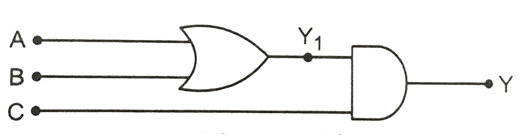
- To get an output y=1 from the circuit shown below, the input must be
Text Solution
|
- Sodium has body centred packing. Distance between two nearest atoms is...
Text Solution
|
- A transistor is operated in common emitter configuration at V(c)=2 V s...
Text Solution
|
- The symbolic representation of four logic gates are given in Fig.The l...
Text Solution
|
- A p-n photodiode is fabricated from a semiconductor with a band gap of...
Text Solution
|
- The circuit is equivalent to
Text Solution
|
- A p-n photodiode is made of a material with a band gap of 2.0 eV. The ...
Text Solution
|
- The voltage gain of an amplifier with 9% negative feedback is 10. The ...
Text Solution
|
- If the lattice parameter for a crystalline structure is 3.6Å, then the...
Text Solution
|
- For a cubic crystal structure which one of the following relations ind...
Text Solution
|
- In the energy band diagram of a material shown below, the open circles...
Text Solution
|
- In the following circuit, the output Y for all possible inputs A and B...
Text Solution
|
- The following figure shows a logic gate circuit with two inputs A and ...
Text Solution
|
- A forward biased diode is
Text Solution
|
- A transistor is operated in common emitter configuration at constant c...
Text Solution
|
- A transistor -oscillator using a resonant circuit with an inductor L (...
Text Solution
|
- Copper has face centred cubic (fc c) lattice with interatomic spacing ...
Text Solution
|
- Choose the only false statement form the following
Text Solution
|