A
B
C
D
Text Solution
Verified by Experts
The correct Answer is:


Topper's Solved these Questions
Similar Questions
Explore conceptually related problems
NEET PREVIOUS YEAR (YEARWISE + CHAPTERWISE)-SOLID AND SEMICONDUCTOR DEVICES-Exercise
- For a cubic crystal structure which one of the following relations ind...
Text Solution
|
- In the energy band diagram of a material shown below, the open circles...
Text Solution
|
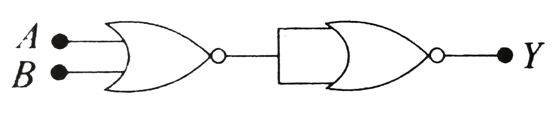
- In the following circuit, the output Y for all possible inputs A and B...
Text Solution
|
- The following figure shows a logic gate circuit with two inputs A and ...
Text Solution
|
- A forward biased diode is
Text Solution
|
- A transistor is operated in common emitter configuration at constant c...
Text Solution
|
- A transistor -oscillator using a resonant circuit with an inductor L (...
Text Solution
|
- Copper has face centred cubic (fc c) lattice with interatomic spacing ...
Text Solution
|
- Choose the only false statement form the following
Text Solution
|
- Carbon , silicon and germanium have four valence elcectrons each . The...
Text Solution
|
- Zener diode is used for
Text Solution
|
- Application of a forward biase to a "p-n" junction:
Text Solution
|
- Of the diodes shown in the following diagrams, which one is reverse bi...
Text Solution
|
- In a "p-n" junction photo cell, the value of the photo electromotive f...
Text Solution
|
- The output of OR gate is 1
Text Solution
|
- The peak voltage in the output of a half-wave diode rectifier fed with...
Text Solution
|
- In semiconductors at a room tempreture
Text Solution
|
- A npn transistor conducts when
Text Solution
|
- If a full wave reactifier circuit is operating from 50 Hz mains, the f...
Text Solution
|
- Barrier potential of a "p-n" junction diode does not depend on
Text Solution
|