A
B
C
D
Text Solution
Verified by Experts
The correct Answer is:


Topper's Solved these Questions
SEMI CONDUCTOR AND LOGIC GATES
MOTION|Exercise EXERCISE 2|33 VideosSEMI CONDUCTOR AND LOGIC GATES
MOTION|Exercise EXERCISE 3|34 VideosROTATIONAL MOTION
MOTION|Exercise Exercise - 3 ( Section-B )|24 VideosSIMPLE HARMONIC MOTION
MOTION|Exercise EXERCISE -3 Section - B Previous Year Problems | JEE MAIN|23 Videos
Similar Questions
Explore conceptually related problems
MOTION-SEMI CONDUCTOR AND LOGIC GATES-EXERCISE 3
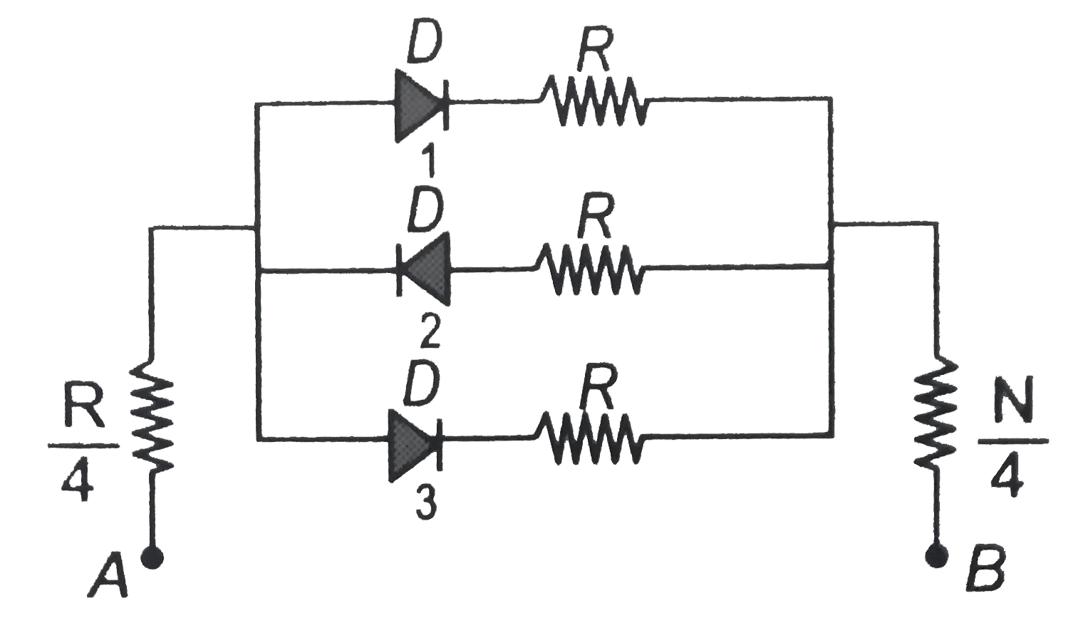
- In the following circuits PN-junction diodes D(1), D(2) and D(3) are i...
Text Solution
|
- If temperature increases, conductivity of semiconductor will be –
Text Solution
|
- At 0K, silicon behave as –
Text Solution
|
- The energy band gap is maximum in
Text Solution
|
- The part of a transistor which is most heavily doped to produce large ...
Text Solution
|
- In the middle of the depletion layer of a reverse - biased p - n junc...
Text Solution
|
- The difference in the variation of resistance with temperature in a me...
Text Solution
|
- A strip of copper and another of germanium are cooled from room tempe...
Text Solution
|
- When n-p-n transistor is used as an amplifier
Text Solution
|
- A piece of copper and another of germanium are cooled from room temper...
Text Solution
|
- The manifestation of band structure in solids is due to
Text Solution
|
- When p-n junction diode is forward biased then
Text Solution
|
- The electrical conductivity of a semiconductor increases when electrom...
Text Solution
|
- In a full wave rectifier circuit operating from 50 Hz mains frequency ...
Text Solution
|
- In a common-base amplifier, the phase difference between the input sig...
Text Solution
|
- If the ratio of the concentration of electron to that of holes in a se...
Text Solution
|
- A solid which is not transperent to visible light and whose conductivi...
Text Solution
|
- In a common base mode of transistor, collector current is 5.488 mA for...
Text Solution
|
- If the lattice constant of this semiconductor is decreased, then which...
Text Solution
|
- In the following, which one of the diodes is reverse biased ?
Text Solution
|
- The circuit has two oppositely connected ideal diodes in parallel. Wha...
Text Solution
|