Text Solution
Verified by Experts


Topper's Solved these Questions
SEMICONDUCTOR ELECTRONICS
SUBHASH PUBLICATION|Exercise FIVE MARKS QUESTIONS WITH ANSWERS|9 VideosSEMICONDUCTOR ELECTRONICS
SUBHASH PUBLICATION|Exercise OPTIONAL NUMERICALS WITH SOLUTIONS|6 VideosSEMICONDUCTOR ELECTRONICS
SUBHASH PUBLICATION|Exercise OPTIONAL NUMERICALS WITH SOLUTIONS|6 VideosRAY OPTICS AND OPTICAL INSTRUMENTS
SUBHASH PUBLICATION|Exercise NUMERICALS WITH SOLUTIONS|22 VideosSUPER MODEL QUESTION PAPER ( WITH ANSWERS )
SUBHASH PUBLICATION|Exercise PART D|26 Videos
Similar Questions
Explore conceptually related problems
SUBHASH PUBLICATION-SEMICONDUCTOR ELECTRONICS-TWO MARKS QUESTIONS WITH ANSWERS
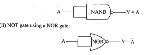
- Represent a NOT gate using a NAND gate or a NOR gate.
Text Solution
|
- Mention any two ways of increasing the conductivity of an intrinsic se...
Text Solution
|
- What are p-type and n-type semiconductors?
Text Solution
|
- Mention the two methods of biasing a diode.
Text Solution
|
- Distinguish between p type and n type semiconductors
Text Solution
|
- Distinguish between n-p-n and p-n-p transistors.
Text Solution
|
- What is a photo diode? In which mode of biasing does it work?
Text Solution
|
- Relate I(E ),I(B) and I(C) for a transistor.
Text Solution
|
- Define current gain at a constant V("CE") and V("BE").
Text Solution
|
- What is meant by input and output resistance of a transistor amplifier...
Text Solution
|
- Mention a few semiconductors employed in the fabrication of solar cell...
Text Solution
|
- Explain a typical p-n juction solar cell with a neat labelling
Text Solution
|
- Draw I-V characteristics of a solar cell.
Text Solution
|
- Draw a labelled diagram for a N-P-N transistor showing the necessary D...
Text Solution
|
- Draw DC bias condition for a PNP transistor.
Text Solution
|
- Show the circuit arrangement for studying the input and output charact...
Text Solution
|
- Draw a neat labelled diagram of a transistor amplifier in a CE mode.
Text Solution
|
- Explain briefly Barkhausen's criteria.
Text Solution
|
- Distinguish between positive feedback and negative feed back.
Text Solution
|
- What is Boolean algebra?
Text Solution
|