Text Solution
Verified by Experts


Topper's Solved these Questions
SEMICONDUCTOR ELECTRONICS
SUBHASH PUBLICATION|Exercise FIVE MARKS QUESTIONS WITH ANSWERS|9 VideosSEMICONDUCTOR ELECTRONICS
SUBHASH PUBLICATION|Exercise OPTIONAL NUMERICALS WITH SOLUTIONS|6 VideosSEMICONDUCTOR ELECTRONICS
SUBHASH PUBLICATION|Exercise OPTIONAL NUMERICALS WITH SOLUTIONS|6 VideosRAY OPTICS AND OPTICAL INSTRUMENTS
SUBHASH PUBLICATION|Exercise NUMERICALS WITH SOLUTIONS|22 VideosSUPER MODEL QUESTION PAPER ( WITH ANSWERS )
SUBHASH PUBLICATION|Exercise PART D|26 Videos
Similar Questions
Explore conceptually related problems
SUBHASH PUBLICATION-SEMICONDUCTOR ELECTRONICS-TWO MARKS QUESTIONS WITH ANSWERS
- Draw I-V characteristics of a solar cell.
Text Solution
|
- Draw a labelled diagram for a N-P-N transistor showing the necessary D...
Text Solution
|
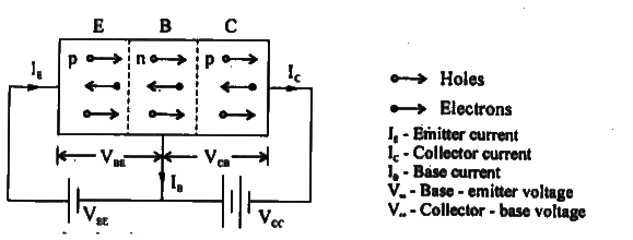
- Draw DC bias condition for a PNP transistor.
Text Solution
|
- Show the circuit arrangement for studying the input and output charact...
Text Solution
|
- Draw a neat labelled diagram of a transistor amplifier in a CE mode.
Text Solution
|
- Explain briefly Barkhausen's criteria.
Text Solution
|
- Distinguish between positive feedback and negative feed back.
Text Solution
|
- What is Boolean algebra?
Text Solution
|
- Give the logic symbol, Boolean expression and truth table of an AND ga...
Text Solution
|
- Write the symbol and truth table for a logic NOT gate
Text Solution
|
- Give the logic symbol, Boolean expression and truth table of a NAND ga...
Text Solution
|
- Give the logic symbol, Boolean expression and truth table of a NOR gat...
Text Solution
|
- Write the Boolean equation for a NOR gate and a NAND gate
Text Solution
|
- Name the two types of integrated circuits.
Text Solution
|
- How are electron-hole pairs created in a semiconductor?
Text Solution
|
- When does electron-hole recombination take place?
Text Solution
|
- Give a schematic two-dimensional representation of an intrinsic Si or ...
Text Solution
|
- Draw energy band diagram of an intrinsic semiconductor at room tempera...
Text Solution
|
- Draw I-V characteristics of a Zener diode with neat labelling.
Text Solution
|
- Draw a neat labelled diagram of a Zener diode used as a DC voltage reg...
Text Solution
|