Text Solution
Verified by Experts


Topper's Solved these Questions
CBSE Examination Paper Delhi–2014
CBSE COMPLEMENTARY MATERIAL|Exercise Set-II (Questions Uncommon to Set-I)|10 VideosCBSE Examination Paper Delhi–2014
CBSE COMPLEMENTARY MATERIAL|Exercise SET-III (Questions Uncommon to set-I and II)|9 VideosCBSE EXAMINATION PAPER - 2016
CBSE COMPLEMENTARY MATERIAL|Exercise SECTION - E|17 VideosCBSE EXAMINATION PAPER, DELHI REGION - 2015 (CODE NO. 55/1/1/D)
CBSE COMPLEMENTARY MATERIAL|Exercise SECTION E|6 Videos
Similar Questions
Explore conceptually related problems
CBSE COMPLEMENTARY MATERIAL-CBSE Examination Paper Delhi–2014-SET-III (Questions Uncommon to set-I and II)
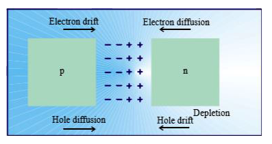
- (a) state briefly the processes involved in the formation of p-n ho...
Text Solution
|
- Define the term 'drift velocity' of charge carriers in a conductor and...
Text Solution
|
- Plot a graph showing variation of current versus voltage for the mater...
Text Solution
|
- An electric dipole of length 1cm, which places with its axis making an...
Text Solution
|
- A proton and alpha particle are accelerated through the same accelerat...
Text Solution
|
- A 12.3 eV electron beam is used to bombard gaseous hydrogen at room te...
Text Solution
|
- Name the em waves which are produced during radioactive decay of a nuc...
Text Solution
|
- Welders wear special glass goggles ro facemask with glass window to pr...
Text Solution
|
- Why are infrared waves often called as heat waves? Give their one appl...
Text Solution
|
- A potentiometer wire of length 1 m has a resistance of 5Omega. It is c...
Text Solution
|