A
B
C
D
Text Solution
Verified by Experts
The correct Answer is:


Topper's Solved these Questions
SEMICONDUCTOR ELECTRONICS : MATERIALS , DEVICES AND SIMPLE CIRCUITS
NCERT FINGERTIPS|Exercise Higher Order Thinking Skills|8 VideosSEMICONDUCTOR ELECTRONICS : MATERIALS , DEVICES AND SIMPLE CIRCUITS
NCERT FINGERTIPS|Exercise NCERT Exemplar|8 VideosSEMICONDUCTOR ELECTRONICS : MATERIALS , DEVICES AND SIMPLE CIRCUITS
NCERT FINGERTIPS|Exercise Junction Transistor|33 VideosRAY OPTICS AND OPTICAL INSTRUMENTS
NCERT FINGERTIPS|Exercise Assertion And Reason|15 VideosWAVE OPTICS
NCERT FINGERTIPS|Exercise Assertion And Reason|15 Videos
Similar Questions
Explore conceptually related problems
NCERT FINGERTIPS-SEMICONDUCTOR ELECTRONICS : MATERIALS , DEVICES AND SIMPLE CIRCUITS -Digital Electronics And Logic Gates
- Boolean algebra is essentially based on
Text Solution
|
- The symbolic representation of four logic gates are given in Fig. The ...
Text Solution
|
- In the circuit below, A and B represents two inputs and C represents t...
Text Solution
|
- Write the truth table for the circuit shown in figure given below. Nam...
Text Solution
|
- In boolean algebra, if A=1 and B=0 then the value of A+barB is
Text Solution
|
- What will be the input of A and B for the Boolean expression bar((A+B)...
Text Solution
|
- दिये गये लॉजिक परिपथ का तुल्य लॉजिक गेट है
Text Solution
|
- The combination of NAND gates is shown in figure. The equivalent circu...
Text Solution
|
- The diagram of a logic circuit is given below. The output F of the cir...
Text Solution
|
- The truth table of the logic circuit shown-
Text Solution
|
- Select the outputs Y of the combination of gates shown below for input...
Text Solution
|
- The given truth table is for which
Text Solution
|
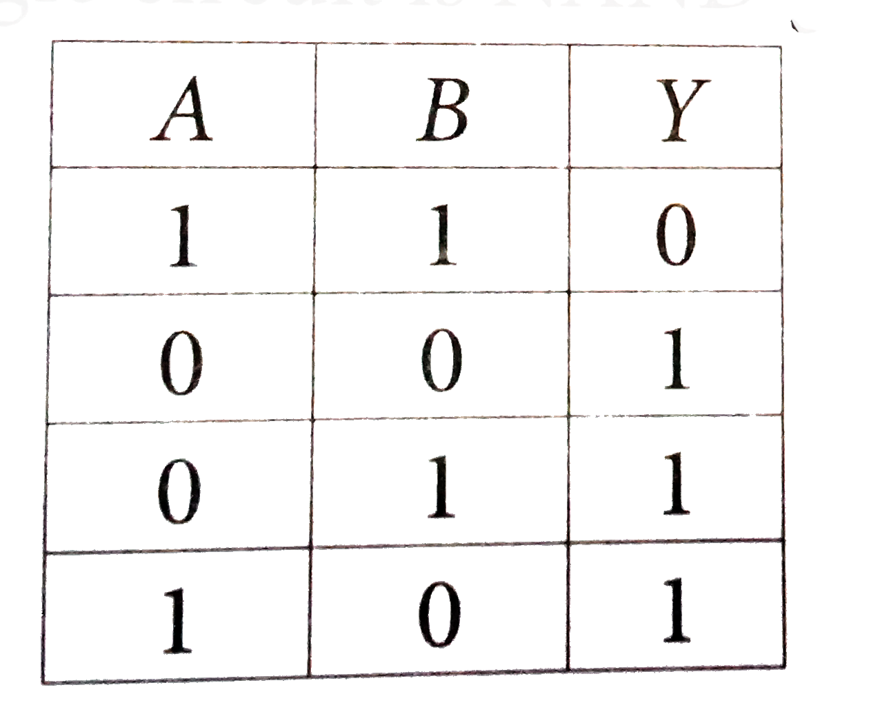
- Which of the following truth tables corresponds to NAND gate ?
Text Solution
|
- The decimal equivalent of the binary number (11010.101)(2) is
Text Solution
|
- The following figure shows a logic gate circuit with two inputs A and ...
Text Solution
|
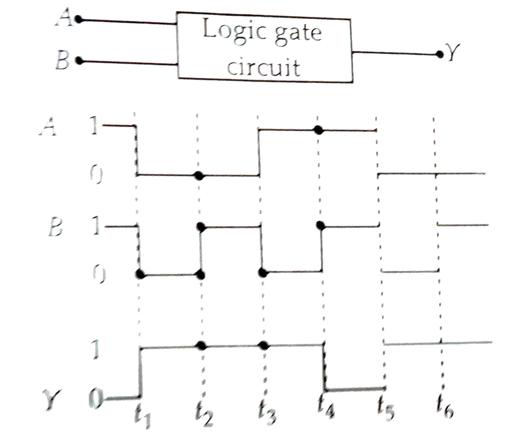
- The logic circuit shown below has the inputs waveforms A and B as show...
Text Solution
|