Home
Class 12
PHYSICS
You are given two circuit as shown in Fi...

You are given two circuit as shown in Fig.and . Which consists of NAND gates. Identify the logic operation carried out by the two circuits.

Text Solution

Verified by Experts

From fig(a). The output of NAND gate is connected to NOT gate (obtained from NAND gate ) Let `y^(1)` be the output of NAND gate and the final output of the combination of two gates is Y. The output of a NAND gate is O only when both the inputs are zero, while in NOT gate, the input gets inverted. Truth table for the arrangement

It is the truth tables of AND gate. Therefore the given circuit acts as AND gate.
(b) The output of two NOT gates are connected to NAND gate Let `Y_(1)andY_(2)` be the outputs of the two NOT gates and the final output of the combination of three gates be Y. In a NOT gate. the input gets inverted, while the output of a NAND gate is .O. only when both the inputs are zero. Truth table for given arrangement.
Promotional Banner

Topper's Solved these Questions

  • SEMICONDUCTOR ELECTRONICS

    NARAYNA|Exercise EVALUATE YOURSELF-1|5 Videos
  • SEMICONDUCTOR ELECTRONICS

    NARAYNA|Exercise EVALUATE YOURSELF-2|3 Videos
  • SEMI CONDUCTOR DEVICES

    NARAYNA|Exercise Level-II (H.W)|36 Videos
  • WAVE OPTICS

    NARAYNA|Exercise Exercise - 4 Polarisation|9 Videos

Similar Questions

Explore conceptually related problems

Identify the logic operation carried out by the following circuit

Identify the logic operation performed by the circuit given here.

In the two circuits shown in figure

In the given circuit (as shown in fig. 5.319).

Identify the operation performed by the circuit given below-

Identify the operation performed by the circuit given below:

Identify the operation performed by the circuit given below :-

Identify the operation performed by the circuit given below :-

Write the truth table for the circuit given in Fig., consisting of NOR gates only. Identify the logic operations (OR, AND, NOT) performed by two circuits.

NARAYNA-SEMICONDUCTOR ELECTRONICS-ADDITIONAL EXERCISE (ASSERTION AND REASON TYPE QUESTIONS :)
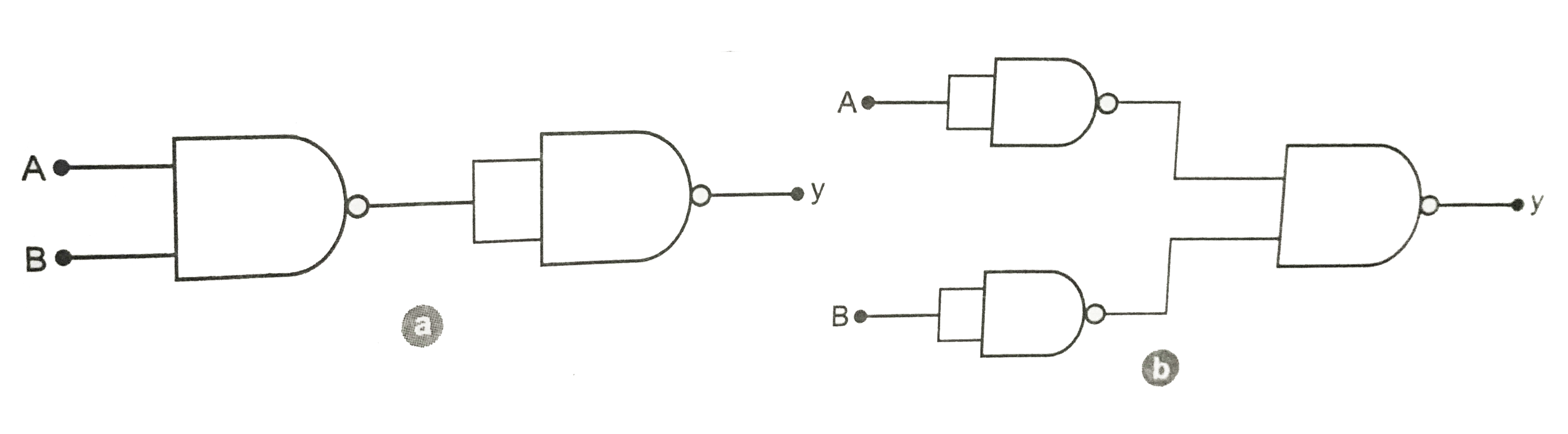
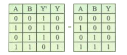
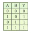
  1. You are given two circuit as shown in Fig.and . Which consists of NAND...

    Text Solution

    |

  2. Assertion : the following circuit represents 'OR' gate Reason : f...

    Text Solution

    |

  3. Assertion : In the following circuit the potential drop across the res...

    Text Solution

    |

  4. Assertion: NOT gate is also called inverter circuit. Reason: NOT gat...

    Text Solution

    |

  5. Assertion: The current gain in common base circuit is always less than...

    Text Solution

    |

  6. Assertion : The dominant mechanism for motion of charge carreis in for...

    Text Solution

    |

  7. Assertion : The value of current through p-n junction in the given fig...

    Text Solution

    |

  8. Statement-I : A p-n junction with reverse bias can be used as a photod...

    Text Solution

    |

  9. Assertion : In common base configuration, the current gain of the tran...

    Text Solution

    |

  10. Statement-I : Germanium is preferred over silicon for making semicondu...

    Text Solution

    |

  11. Assertion : The temparature coefficient of resistance is positive for ...

    Text Solution

    |

  12. Assertion : For a given applied voltage, conduction current in n-type ...

    Text Solution

    |

  13. Assertion : We cannot meausre that potential barrier of p-n junction b...

    Text Solution

    |

  14. Assertion : In Zener diode depletion layer is thin. Reason : In rev...

    Text Solution

    |

  15. Statement-I : A p-n junction with reverse bias can be used as a photod...

    Text Solution

    |

  16. Statement-I : When base region has larger width, the collector current...

    Text Solution

    |

  17. Statement-I : To be used as amplifier, the transistor in the common em...

    Text Solution

    |

  18. Assertion : A transistor amplifier operates in active region. Reason...

    Text Solution

    |

  19. Assertion: NAND or NOR gates are called digital building blocks. Rea...

    Text Solution

    |

  20. Assertion : In transistor, common emitter configuration is used to mak...

    Text Solution

    |