A
B
C
D
Text Solution
Verified by Experts
The correct Answer is:


Topper's Solved these Questions
SEMICONDUCTOR ELECTRONICS
NARAYNA|Exercise C.U.Q (APPLICATION OF JUNCTION DIODE AS RECTIFIER)|7 VideosSEMICONDUCTOR ELECTRONICS
NARAYNA|Exercise C.U.Q (SPECIAL PURPOSE P-N JUNCTION DIODES)|51 VideosSEMICONDUCTOR ELECTRONICS
NARAYNA|Exercise EVALUATE YOURSELF-4|5 VideosSEMI CONDUCTOR DEVICES
NARAYNA|Exercise Level-II (H.W)|36 VideosWAVE OPTICS
NARAYNA|Exercise Exercise - 4 Polarisation|9 Videos
Similar Questions
Explore conceptually related problems
NARAYNA-SEMICONDUCTOR ELECTRONICS-C.U.Q (INTRINSIC AND EXTRINSIC SEMICONDUCTORS)
- The thickness of depletion layer is approximately
Text Solution
|
- The depletion region is
Text Solution
|
- Diffusion current in a p-n junction is greater than the drift current ...
Text Solution
|
- Diode is forward biased and the applied voltage is greater than the po...
Text Solution
|
- When a junction diode is reverse biased, then current called drift cur...
Text Solution
|
- Among the following one statement is not correct when a junction diode...
Text Solution
|
- Consider the following statement A and B and identify the correct choi...
Text Solution
|
- The potential in the depletion layer due to.
Text Solution
|
- Pickout the incorrect statement regarding reverse saturation current i...
Text Solution
|
- When the p-n junction diode is reverse biased, the thickness of the de...
Text Solution
|
- p-n junction diode can be used as
Text Solution
|
- A p-n junction diode is reverse biased. Then
Text Solution
|
- In the middle of the depletion layer of a reverse - biased p - n junc...
Text Solution
|
- When p-n junction diode is forward biased then
Text Solution
|
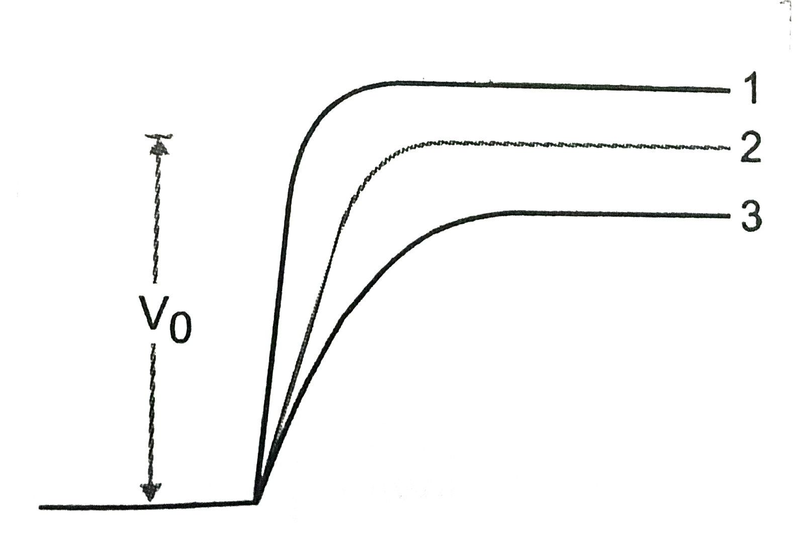
- In Fig . V(0) is the potential barrier across a p-n junction, when no ...
Text Solution
|
- In Fig assuming the diodes to be ideal :
Text Solution
|
- A Si and a Ge diode has identical physical dimensions. The band gap in...
Text Solution
|
- The correct curve between potential (V) and distance (d) near p-n junc...
Text Solution
|
- Which of the following is reverse biased diode?
Text Solution
|
- In the case of forward biasing of PN-junction, which one of the follow...
Text Solution
|