A
B
C
D
Text Solution
Verified by Experts
The correct Answer is:


Topper's Solved these Questions
SEMICONDUCTOR ELECTRONICS
NARAYNA|Exercise EXERCISE-4|35 VideosSEMICONDUCTOR ELECTRONICS
NARAYNA|Exercise ADDITIONAL EXERCISE (ASSERTION AND REASON TYPE QUESTIONS :)|19 VideosSEMICONDUCTOR ELECTRONICS
NARAYNA|Exercise EXERCISE -2 (H.W) (LOGIC GATE)|6 VideosSEMI CONDUCTOR DEVICES
NARAYNA|Exercise Level-II (H.W)|36 VideosWAVE OPTICS
NARAYNA|Exercise Exercise - 4 Polarisation|9 Videos
Similar Questions
Explore conceptually related problems
NARAYNA-SEMICONDUCTOR ELECTRONICS-EXERCISE -3
- The input resistance of a silicon transistor is 100 Omega. Base curren...
Text Solution
|
- The figure shows a logic circuit with two inputs A and B and the outpu...
Text Solution
|
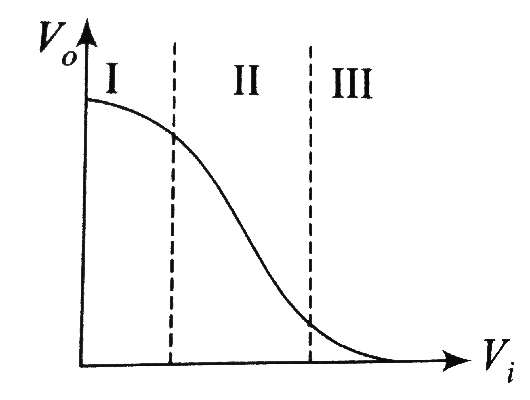
- Transfer characterstics [output voltage (V(o)) vs. input voltage (V(i)...
Text Solution
|
- C and Si both have same lattice structure, having 4 bonding electrons ...
Text Solution
|
- In a CE transistor amplifier, the audio signal voltage across the coll...
Text Solution
|
- Two ideal diodes are connected to a battery as shown in the circuit. T...
Text Solution
|
- A zener diode, having breakdown voltage equal to 15 V is used in a vol...
Text Solution
|
- Pure Si at 500K has equal number of electron (n(e)) and hole (n(h)) co...
Text Solution
|
- In the following figure, the diodes, which are forward biased, are
Text Solution
|
- If a small amount of antimony is added to germanium crystal
Text Solution
|
- Symbolic representation of four logic gates are shown as
Text Solution
|
- In forward biasing of the p-n junction:
Text Solution
|
- A transistor is operated in common emitter configuration at V(c)=2 V s...
Text Solution
|
- To get an output y=1 from the circuit shown below, the input must be
Text Solution
|
- The device that can act as a complete electronic circuit is
Text Solution
|
- Which one of the following bonds produces a solid that reflects light ...
Text Solution
|
- Which one of the following statement is false?
Text Solution
|
- Sodium has body centred packing. Distance between two nearest atoms is...
Text Solution
|
- The number of beta particles emitter by radioactive sustance is twice ...
Text Solution
|
- A transistor is operated in common emitter configuration at V(c)=2 V s...
Text Solution
|