A
B
C
D
Text Solution
Verified by Experts
The correct Answer is:


Topper's Solved these Questions
SEMICONDUCTOR ELECTRONICS
NARAYNA|Exercise EXERCISE-4|35 VideosSEMICONDUCTOR ELECTRONICS
NARAYNA|Exercise ADDITIONAL EXERCISE (ASSERTION AND REASON TYPE QUESTIONS :)|19 VideosSEMICONDUCTOR ELECTRONICS
NARAYNA|Exercise EXERCISE -2 (H.W) (LOGIC GATE)|6 VideosSEMI CONDUCTOR DEVICES
NARAYNA|Exercise Level-II (H.W)|36 VideosWAVE OPTICS
NARAYNA|Exercise Exercise - 4 Polarisation|9 Videos
Similar Questions
Explore conceptually related problems
NARAYNA-SEMICONDUCTOR ELECTRONICS-EXERCISE -3
- In forward biasing of the p-n junction:
Text Solution
|
- A transistor is operated in common emitter configuration at V(c)=2 V s...
Text Solution
|
- To get an output y=1 from the circuit shown below, the input must be
Text Solution
|
- The device that can act as a complete electronic circuit is
Text Solution
|
- Which one of the following bonds produces a solid that reflects light ...
Text Solution
|
- Which one of the following statement is false?
Text Solution
|
- Sodium has body centred packing. Distance between two nearest atoms is...
Text Solution
|
- The number of beta particles emitter by radioactive sustance is twice ...
Text Solution
|
- A transistor is operated in common emitter configuration at V(c)=2 V s...
Text Solution
|
- A p-n photodiode is fabricated from a semiconductor with a band gap of...
Text Solution
|
- The circuit is equivalent to
Text Solution
|
- A p-n photodiode is made of a material with a band gap of 2.0 eV. The ...
Text Solution
|
- The voltage gain of an amplifier with 9% negative feedback is 10. The ...
Text Solution
|
- In the energy band diagram of a material shown below, the open circles...
Text Solution
|
- For a cubic crystal structure which one of the following relations ind...
Text Solution
|
- A common emitter amplifier has a voltage gain of 50, an input impedanc...
Text Solution
|
- In the following circuit, the output Y for all possible inputs A and B...
Text Solution
|
- A forward biased diode is
Text Solution
|
- A transistor is operated in common emitter configuration at constant c...
Text Solution
|
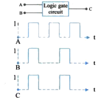
- The following figure shown a logic gate circuit with ttwo inputs A and...
Text Solution
|