Text Solution
Verified by Experts


Topper's Solved these Questions
SEMICONDUCTOR ELECTRONICS (MATERIAL, DEVICES AND SIMPLE CIRUITS )
AAKASH INSTITUTE|Exercise EXERCISE|13 VideosSEMICONDUCTOR ELECTRONICS (MATERIAL, DEVICES AND SIMPLE CIRUITS )
AAKASH INSTITUTE|Exercise Assignment section -A (Objective Type Question)|38 VideosSEMICONDUCTOR ELECTRONICS (MATERIAL, DEVICES AND SIMPLE CIRUITS )
AAKASH INSTITUTE|Exercise Assignment SECTION - D (Assertion & reason type Question)|10 VideosRAY OPTICS AND OPTICAL INSTRUMENTS
AAKASH INSTITUTE|Exercise ASSIGNMENT (SECTION - D)|16 VideosSEMICONDUCTOR ELECTRONICS: MATERIALS, DEVICES AND SIMPLE CIRCUITS
AAKASH INSTITUTE|Exercise Assignment (Section-D (Assertion and reason))|5 Videos
Similar Questions
Explore conceptually related problems
AAKASH INSTITUTE-SEMICONDUCTOR ELECTRONICS (MATERIAL, DEVICES AND SIMPLE CIRUITS )-TRY YOUR SELF
- A semiconductor is known to have an electron concentration of 6xx10^(1...
Text Solution
|
- Suppose a pure Si-crystal has 5xx10^(28) "atoms" m^(-3). It is doped b...
Text Solution
|
- If in p-n junction diode a sinusoidal input signal is applied as shown...
Text Solution
|
- In a reverse biased diode, when the applied voltage changes by 1V, the...
Text Solution
|
- Potential drop across forward junction p-n diode is 0.7 V. If a batter...
Text Solution
|
- In a semi conductor diode , the barrier potential offers opposition to...
Text Solution
|
- How is forward biasing different from reverse biasing in a p-n junctio...
Text Solution
|
- Application of a forward biase to a p-n junction:
Text Solution
|
- In a p-n junction having depletion layer of thickness 10^(-6) m the po...
Text Solution
|
- Pickout the incorrect statement regarding reverse saturation current i...
Text Solution
|
- In a full -wave rectifier circuit operating from 50 Hz mains frequency...
Text Solution
|
- Freuency of given AC signal is 50 Hz. When it connected to a half - wa...
Text Solution
|
- The output form of full-wave rectifier is
Text Solution
|
- The current in the forward bias is unknown to be more (~mA) than the c...
Text Solution
|
- Why are Si and Ga As preffered materials for solar cells?
Text Solution
|
- For a CE transistor amplifier, the audio signal voltage across the col...
Text Solution
|
- In common emitter transistor as shown in Fig., the V(BB) supply can be...
Text Solution
|
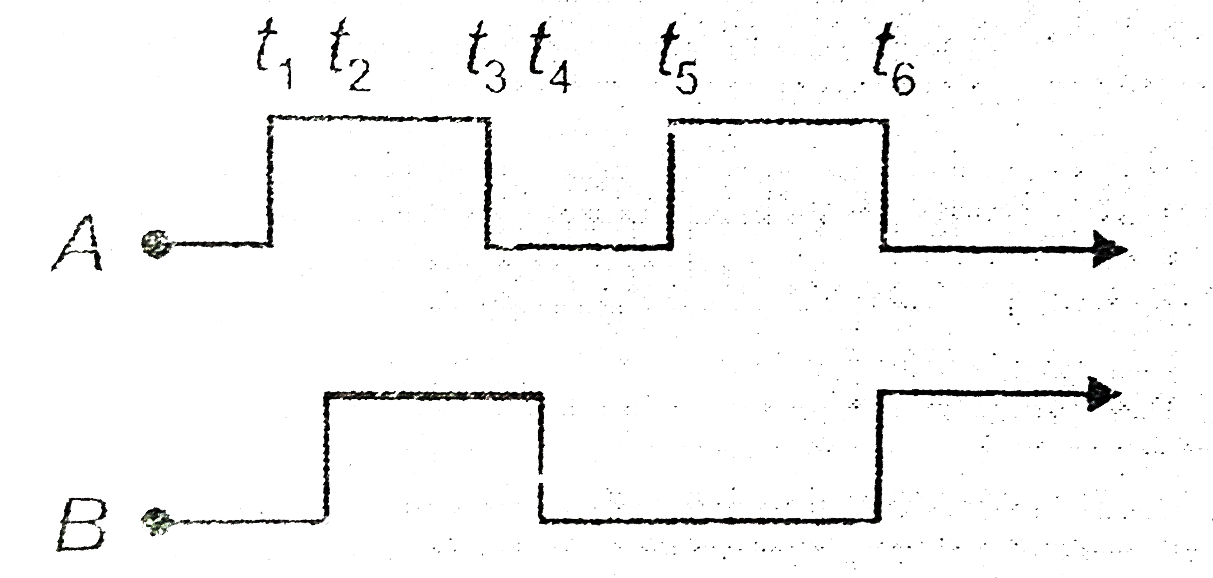
- Show the output waveform of OR gate for the following input waveforms ...
Text Solution
|
- Sketch the output waveform obtained from AND gate for the following in...
Text Solution
|
- Sketch the output waveform Y from a NAND gate having following inputs ...
Text Solution
|