A
B
C
D
Text Solution
Verified by Experts
The correct Answer is:


Topper's Solved these Questions
Similar Questions
Explore conceptually related problems
SIA PUBLICATION-SEMICONDUCTOR ELECTRONICS-MCQ
- A piece of aluminium and germanium each are cooled from T(1)K to T(2)K...
Text Solution
|
- When a p-n junction diode is reverse biased, the thickness of the depl...
Text Solution
|
- Energy band gap E(g) in an insulator is of the order of
Text Solution
|
- Indium impurity in germanium makes it into a
Text Solution
|
- In an intrinsic semiconductor at room temperature number of electrons ...
Text Solution
|
- In forward bias in a p-n junction, the potential barrier
Text Solution
|
- In a reverse biased condition of a p-n junction
Text Solution
|
- Which one of the following is an incorrect statement?
Text Solution
|
- Covalent bond exists in
Text Solution
|
- In a p-type semiconductor, the electrical conduction is due to
Text Solution
|
- To obtain p-type extrinsic semiconductor, the impurity element to be a...
Text Solution
|
- If a battery is connected across a p-n junction with p-type connected ...
Text Solution
|
- The majority carriers in a p-type semiconductor are
Text Solution
|
- If an intrinsic semiconductor a pentavalent element is added as impuri...
Text Solution
|
- In an intrinsic semiconductor the charge carriers responsible for elec...
Text Solution
|
- A semiconductor device which is used for detecting light intensity is ...
Text Solution
|
- A piece of aluminium and germanium each are cooled from T(1)K to T(2)K...
Text Solution
|
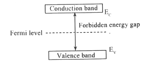
- The energy level stationed at the centre of forbidden energy gap of an...
Text Solution
|
- The method of connecting the negative pole of battery to p-material an...
Text Solution
|
- When boron is added as impurity to silicon, the resulting material is
Text Solution
|