Text Solution
Verified by Experts


Topper's Solved these Questions
SOLIDS AND SEMICONDUCTOR DEVICES
MBD -HARYANA BOARD|Exercise Long answer type questions|6 VideosSOLIDS AND SEMICONDUCTOR DEVICES
MBD -HARYANA BOARD|Exercise Objective type questions|21 VideosSOLIDS AND SEMICONDUCTOR DEVICES
MBD -HARYANA BOARD|Exercise Objective type questions|21 VideosPRINCIPLES OF COMMUNICATION
MBD -HARYANA BOARD|Exercise Objective Type Questions|19 Videos
Similar Questions
Explore conceptually related problems
MBD -HARYANA BOARD-SOLIDS AND SEMICONDUCTOR DEVICES-Short answer type questions
- Define current gain alpha and beta for a transistor. How are they mutu...
Text Solution
|
- Define current gain in common base and common emitter amplifier and fi...
Text Solution
|
- Derive relation between current gain in common base and common-emitter...
Text Solution
|
- Why is common emitter amplifier preferred over common base amplifier?
Text Solution
|
- Draw a labelled diagram using zener diode for constant voltage power s...
Text Solution
|
- What do you understand by potential barrier ?
Text Solution
|
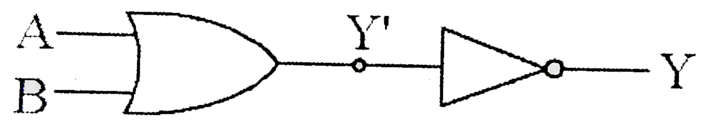
- Name the gate obtained from the combination of gates shown in the figu...
Text Solution
|
- Write the truth table for the circuit given in the figure.
Text Solution
|
- Name the gate obtained from the combination of gates shown in the figu...
Text Solution
|
- Can two p-junction diodes placed back to back act as a p-n-p transisto...
Text Solution
|
- What is the difference between hole current and electron current ?
Text Solution
|
- A n-type semiconductor has a large number of free electrons but still ...
Text Solution
|
- In a transistor, base is made very thin.Explain.
Text Solution
|
- Draw the V-I characterisitics of p-n junction diode in forward bias an...
Text Solution
|
- Draw the I-V characteristics of a zener diode also sketch the circuit ...
Text Solution
|
- Write the truth table for given circuit.
Text Solution
|
- What is doping ? Why is it essential ? What are different dopants used...
Text Solution
|
- How NOR gate is formed ? Draw symbol and truth table for it.
Text Solution
|
- Explain the formation of a NOR gate. Draw its symbol and truth table.
Text Solution
|
- Name of gate obtained from the combination of gates shown in the figur...
Text Solution
|