A
B
C
D
Text Solution
Verified by Experts
The correct Answer is:


Topper's Solved these Questions
SEMICONDUCTOR ELECTRONICS METERIALS DEVICES AND SIMPLE CIRCUITS
MODERN PUBLICATION|Exercise COMPETION FILE (JEE(MAIN) & OTHER STATE BOARDS FOR ENGINEERING ENTRANCE )|31 VideosSEMICONDUCTOR ELECTRONICS METERIALS DEVICES AND SIMPLE CIRCUITS
MODERN PUBLICATION|Exercise COMPETION FILE( MULTIPLE CHOICE QUESTIONS )|17 VideosSEMICONDUCTOR ELECTRONICS METERIALS DEVICES AND SIMPLE CIRCUITS
MODERN PUBLICATION|Exercise REVISION EXERCISES (NUMERICAL PROBLEMS )|15 VideosRAY OPTICS AND OPTICAL INSTRUMENTS
MODERN PUBLICATION|Exercise CHAPTER PRACTICE TEST|14 VideosWAVE OPTICAL
MODERN PUBLICATION|Exercise CHAPTER PRACTICE TEST|7 Videos
Similar Questions
Explore conceptually related problems
MODERN PUBLICATION-SEMICONDUCTOR ELECTRONICS METERIALS DEVICES AND SIMPLE CIRCUITS -COMPETION FILE (MULTIPLE CHOICE QUESTIONS WITH ONLY ONE CORRECT ANSWER)
- For a p-type semiconductor, which of the following statements is true?
Text Solution
|
- The correct booleon operation represented by the circuit diagram dra...
Text Solution
|
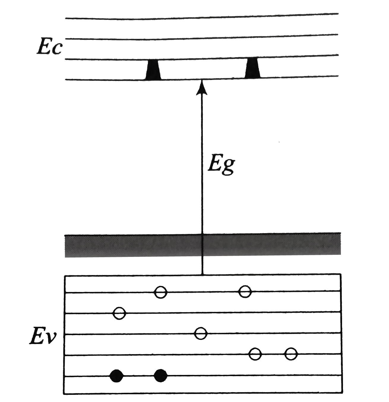
- In the energy band diagram of a material shown below, the open circles...
Text Solution
|
- In the circuit shown in the figure, the input voltage V(i) is 20V,V(BE...
Text Solution
|
- In a p-n junction diode, change in temperature due to heating
Text Solution
|
- In the combination of the following gates the output Y can be written ...
Text Solution
|
- A light emitting diode (LED) has a voltage drop of 2V across it and pa...
Text Solution
|
- A p-n photodiode is made of a material with a band gap of 2.0 eV. The ...
Text Solution
|
- A p-n photodiode is fabricated from a semiconductor with a band gap of...
Text Solution
|
- A transistor is operated in common emitter configuration at V(c)=2 V s...
Text Solution
|
- A common emitter amplifier has a voltage gain of 50, an input impedanc...
Text Solution
|
- If a small amount of antimony is added to germanium crystal
Text Solution
|
- Transfer characteristics vs input volage for a base biased transist...
Text Solution
|
- C and Si both have same lattice structure, having 4 bonding electrons ...
Text Solution
|
- The figure shows a logic circuit with two inputs A and B and the outpu...
Text Solution
|
- In a common emitter (CE) amplifier having a voltage gain G, the transi...
Text Solution
|
- The ouptu x of the logic circuit will be
Text Solution
|
- The given graph represents V-I characteristic for a semiconductor dev...
Text Solution
|
- The barrier potential of a p-n junction depends on : (a) type of semic...
Text Solution
|
- Consider the juction diode as ideal the value of current flowing th...
Text Solution
|