A
B
C
D
Text Solution
Verified by Experts
The correct Answer is:


Topper's Solved these Questions
SEMICONDUCTOR AND DEVICE
FIITJEE|Exercise SOLVED PROBLEMS Objective: Level-I|20 VideosSEMICONDUCTOR AND DEVICE
FIITJEE|Exercise ASSIGNMENT PROBLEMS( objective : Level-I)|41 VideosROTATIONAL MECHANICS
FIITJEE|Exercise COMPREHENSION - IV|2 VideosSIMPLE HARMONIC MOTION
FIITJEE|Exercise Assignment Problems (Objective) (Level-II)|20 Videos
Similar Questions
Explore conceptually related problems
FIITJEE-SEMICONDUCTOR AND DEVICE-ASSIGNMENT PROBLEMS( objective : Level-II)
- If a p-n junction diode is reverse biased, then the resistance measure...
Text Solution
|
- A common emitter transistor amplifier has a current gain of 50. If the...
Text Solution
|
- The current gain of a transistor in a common emitter circuit is 40.The...
Text Solution
|
- The current gain for transistor working as a common base amplifier i...
Text Solution
|
- In an intrinsic semiconductor at room temperature, number of electrons...
Text Solution
|
- If the two ends p and n of a p-n diode junction are joined by a wire, ...
Text Solution
|
- The valence band and conduction band of a solid overlap at low tempera...
Text Solution
|
- The diode used in the circuit shown in the adjacent figure has a const...
Text Solution
|
- A semiconductor X is made by dopping a germanium crystal with arsenic ...
Text Solution
|
- A common-emitter amplifier is designed with an n-p-n transistor (alpha...
Text Solution
|
- The dominant mechanisms for motion of charge carriers in forward and r...
Text Solution
|
- If the forward voltage in a semiconductor is doubled, the width of dep...
Text Solution
|
- In a transistor circuit, when the base current is increased by 50mu A ...
Text Solution
|
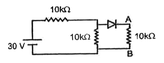
- In the adjacent figure, the potential difference between A and B is
Text Solution
|
- From the following transistor characteristics, what can be inferred?
Text Solution
|
- In Question 26, for VCE=0 the above graph lines will be
Text Solution
|
- What can be said from graph below?
Text Solution
|
- If critical frequency is 20 MHz for ionosphere, calculate the angle of...
Text Solution
|
- A carrier wave of amplitude A is used to modulate (amplitude) the sign...
Text Solution
|
- Which of the following is not a transducer?
Text Solution
|