Text Solution
Verified by Experts


Similar Questions
Explore conceptually related problems
Recommended Questions
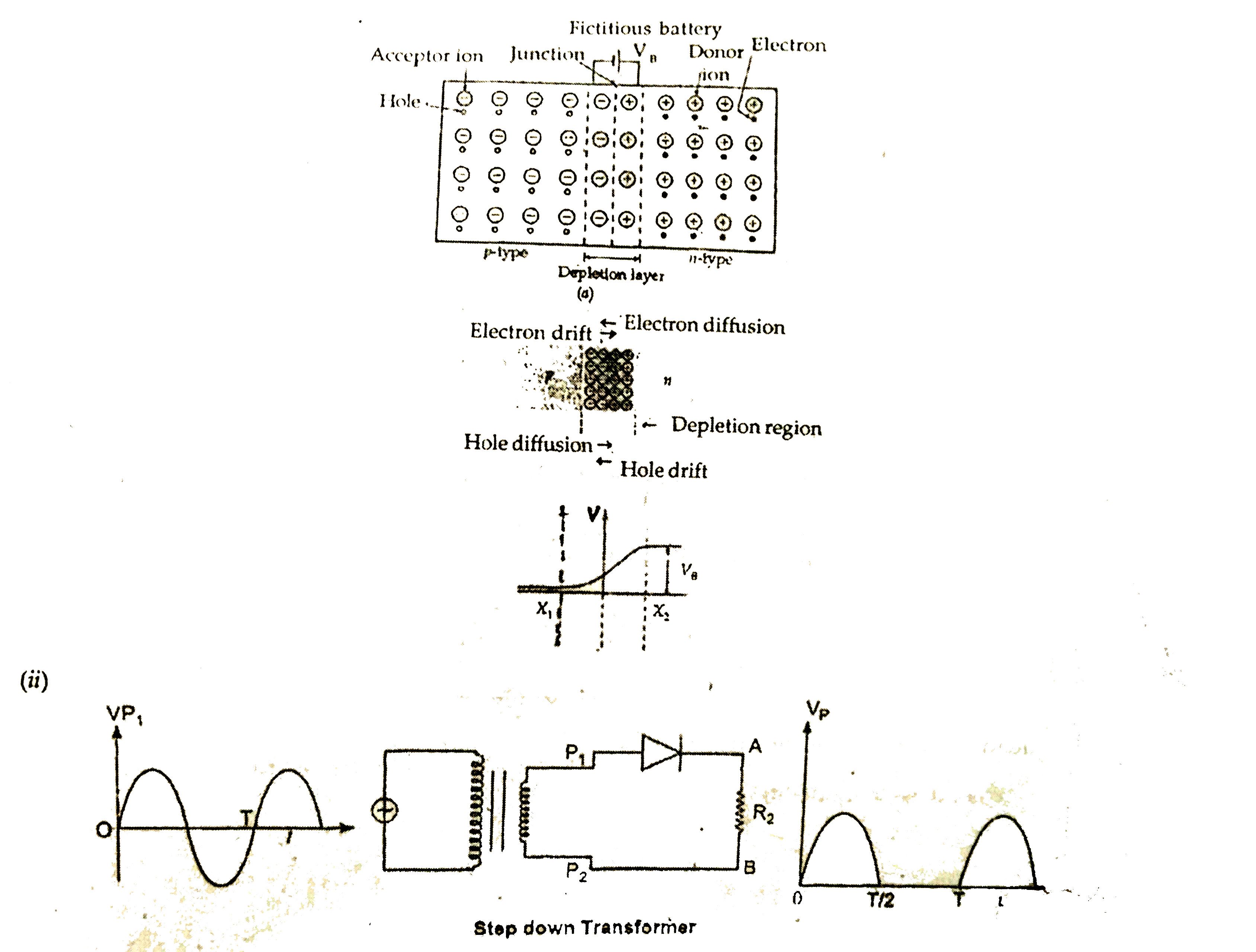
- Explain the formation of depletion layer and potential barrier in p-n ...
Text Solution
|
- Explain the formation of depletion layer and potential barrier in p-n ...
Text Solution
|
- Explain with the help of a circuit diagram, the working of a p-n junct...
Text Solution
|
- Draw the circuit diagram of a half wave rectifier and explain its work...
Text Solution
|
- With the help of circuit diagram explain, the working of p-n junction ...
Text Solution
|
- Draw the circuit diagram of a half wave rectifier and explain its work...
Text Solution
|
- Draw the circuit diagram of a half wave rectifier and explain its work...
Text Solution
|
- (a) Define the terms depletion layer and barrier potential for a p-n ...
Text Solution
|
- Explain with the help of a diagram the formation of depletion layer an...
Text Solution
|