Text Solution
Verified by Experts


Topper's Solved these Questions
Similar Questions
Explore conceptually related problems
XII BOARDS PREVIOUS YEAR-XII BOARDS-SECTION - E
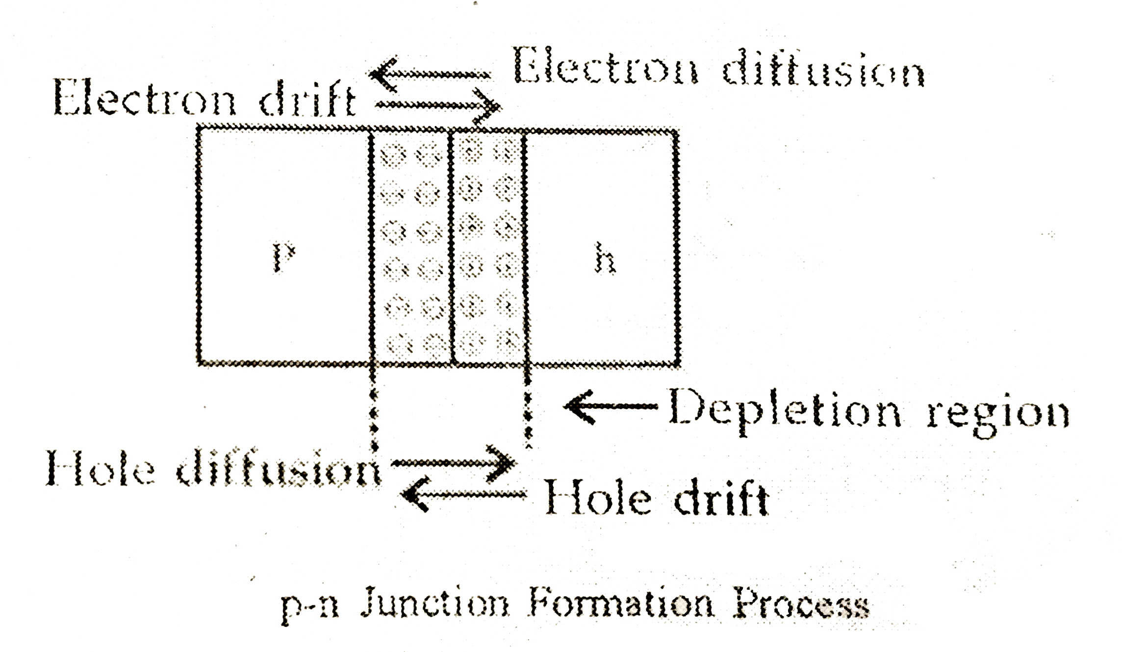
- (a) Explain with the help of suitable diagram , the two processes whic...
Text Solution
|
- (a) Describe briefly three factors which justify the need for modula...
Text Solution
|
- Two point charges q and - q are located at points (0 , 0 , - a ) and ...
Text Solution
|
- A capacitor of capacitance C(1) is charged to a potential V(1) while ...
Text Solution
|
- (a) Draw graphs showing the variations of inductive reactnace and cap...
Text Solution
|
- State the principle of working of a transformer. (b) Define effi...
Text Solution
|