Text Solution
Verified by Experts


Topper's Solved these Questions
SEMICONDUCTOR ELECTRONICS : MATERIALS, DEVICES AND SIMPLE CIRCUITS
KUMAR PRAKASHAN|Exercise Section-B : Numericals (Numerical From Textual Exercise)|15 VideosSEMICONDUCTOR ELECTRONICS : MATERIALS, DEVICES AND SIMPLE CIRCUITS
KUMAR PRAKASHAN|Exercise Section-B : Numericals (Numerical From .DARPAN. Based On Textbook)|14 VideosSEMICONDUCTOR ELECTRONICS : MATERIALS, DEVICES AND SIMPLE CIRCUITS
KUMAR PRAKASHAN|Exercise Section-A : Questions - Answers|51 VideosSAMPLE QUESTION PAPER
KUMAR PRAKASHAN|Exercise PART-B SECTION-C|5 VideosWAVE OPTICS
KUMAR PRAKASHAN|Exercise SECTION-D (MULTIPLCE CHOICE QUESTIONS (MCQS)) (MCQS FROM DARPAN BASED ON TEXTBOOK)|239 Videos
Similar Questions
Explore conceptually related problems
KUMAR PRAKASHAN-SEMICONDUCTOR ELECTRONICS : MATERIALS, DEVICES AND SIMPLE CIRCUITS -Section-B : Numericals (Numerical From Textual illustrations)
- C, Si and Ge have same lattice structure. Why is C insulator while Si ...
Text Solution
|
- Sn, Si and Ge have the same lattice structure . Why Sn is a conductor...
Text Solution
|
- Suppose a pure Si crystal has 5xx10^(28) atoms m^(-3). It is doped by...
Text Solution
|
- At temperature 300 K number density of electrons and holes in pure sil...
Text Solution
|
- Can we take one slab of p-type semiconductor and physically join it to...
Text Solution
|
- The V to I characteristic of a silicon diode is shown in the figure. C...
Text Solution
|
- The values of voltage V and current I for a given diode are given in ...
Text Solution
|
- In a Zener regulated power supply a Zener diode with V(Z)=6.0V is used...
Text Solution
|
- The current in the forward bias is known to be more (~mA) than the cur...
Text Solution
|
- Why are Si and GaAs are perferred materials for solar cells?
Text Solution
|
- Justify the output waveform (Y) of the OR gate for the following input...
Text Solution
|
- The digital signal for the OR gate with two inputs is shown in the fig...
Text Solution
|
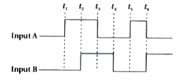
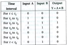
- As shown in the following figure, take A and B input waveforms. Sketch...
Text Solution
|
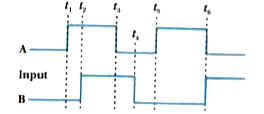
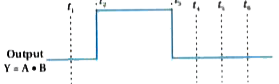
- As shown in the following figure, take A and B input waveforms. Sketch...
Text Solution
|
- Justify the output waveform (Y) of the OR gate for the following input...
Text Solution
|
- As shown in the following figure take A and B input waveforms. Sketch...
Text Solution
|