Home
Class 12
PHYSICS
The following figure shows a logic gate ...

The following figure shows a logic gate circuit with two inputs `A` and `B` and the output `Y`. The voltage waveforms of `A,B` and the output `Y` are as given

A

NOR gate

B

OR gate

C

AND gate

D

NAND gate

Text Solution

Verified by Experts

The correct Answer is:
D

It is clear from given logic circuit, that output Y is low when both the inputs are high, otherwise it is high. Thus, logic circuit is NAND gate.
`|{:(A,B,Y),(1,1,0),(0,0,1),(0,1,1),(1,0,1):}|`
Promotional Banner

Topper's Solved these Questions

  • ELECTRONIC DEVICES

    MTG GUIDE|Exercise CHECK YOUR BEET VITALS|25 Videos
  • ELECTROMAGNETIC WAVES

    MTG GUIDE|Exercise AIPMT/NEET(MCQs)|15 Videos
  • ELECTROSTATICS

    MTG GUIDE|Exercise AIPMT/NEET (MCQ.s)|34 Videos

Similar Questions

Explore conceptually related problems

The following figure shows a logic gate circuit with two inputs A and B and the output C . The voltage waveforms of A,B and C are as shown below

The following figure shows a logic gate circuit with two inputs A and B and the output Y. The voltage waveforms of A,B and Y are as given : The logic gate is

The following figure showns a AND logic gate circuit with two inputs A and B and the output C. The voltage waveforms at C will be -

The following figure shows a logic gate circuit with two inputs A and B and the output C. The voltage waveforms of A, B and C are as shown below. The logic circuit gate is

The following figure shows a logic gate circuit with two inputs A and B output C. The voltage waveforms of A,B and C are as shown in second figure given below :- The logic circuit gate is :-

The following shows a logic gate circuit with two inputs A and B and the output C. The voltage waveforms of A, B and C are as shown below. The logic circuit gate is

The figure shows a logic circuit with two inputs A and B and the output C . The voltage wave forms across A,B and C are as given. The logic circuit gate is

MTG GUIDE-ELECTRONIC DEVICES-AIPMT/NEET (MCQs)
  1. A common emitter amplifier has a voltage gain of 50, an input impedanc...

    Text Solution

    |

  2. To get an output y=1 from the circuit shown below, the input must be

    Text Solution

    |

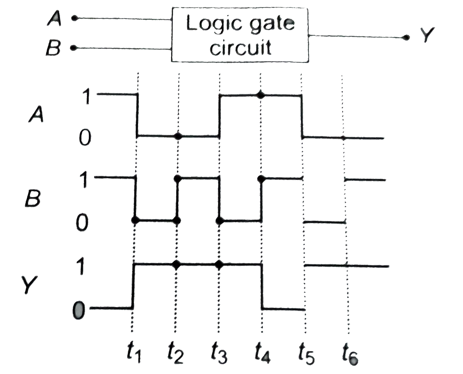
  3. The following figure shows a logic gate circuit with two inputs A and ...

    Text Solution

    |

  4. For transistor action: (1) Base, emitter and collector regions shoul...

    Text Solution

    |

  5. A transistor is operated in common emitter configuration at V(c)=2 V s...

    Text Solution

    |

  6. In forward biasing of the p-n junction

    Text Solution

    |

  7. Symbolic representation of four logic gates are shown as: Pick ou...

    Text Solution

    |

  8. If a small amount of antimony is added to germanium crystal

    Text Solution

    |

  9. A zener diode, having breakdown voltage equal to 15 V is used in a vol...

    Text Solution

    |

  10. In the following figure, the diodes which are forward biased are:

    Text Solution

    |

  11. Pure Si at 500K has equal number of electron (n(e)) and hole (n(h)) co...

    Text Solution

    |

  12. Two ideal diodes are connected to a battery as shown in the circuit. T...

    Text Solution

    |

  13. In a CE transistor amplifier, the audio signal voltage across the coll...

    Text Solution

    |

  14. C and Si both have same lattice structure, having 4 bonding electrons ...

    Text Solution

    |

  15. The figure shows a logic circuit with two inputs A and B and the outpu...

    Text Solution

    |

  16. The input resistance of a silicon transistor is 100 Omega. Base curren...

    Text Solution

    |

  17. To get an output Y = 1 in given circuit, which of the following input ...

    Text Solution

    |

  18. In a common emitter (CE) amplifier having a voltage gain G, the transi...

    Text Solution

    |

  19. In a n-type semiconductor, which of the following statement is true?

    Text Solution

    |

  20. The output (X) of the logic circuit shown in figure will be

    Text Solution

    |