A
B
C
D
Text Solution
Verified by Experts
The correct Answer is:


Topper's Solved these Questions
Similar Questions
Explore conceptually related problems
MTG GUIDE-ELECTRONIC DEVICES-AIPMT/NEET (MCQs)
- In a CE transistor amplifier, the audio signal voltage across the coll...
Text Solution
|
- C and Si both have same lattice structure, having 4 bonding electrons ...
Text Solution
|
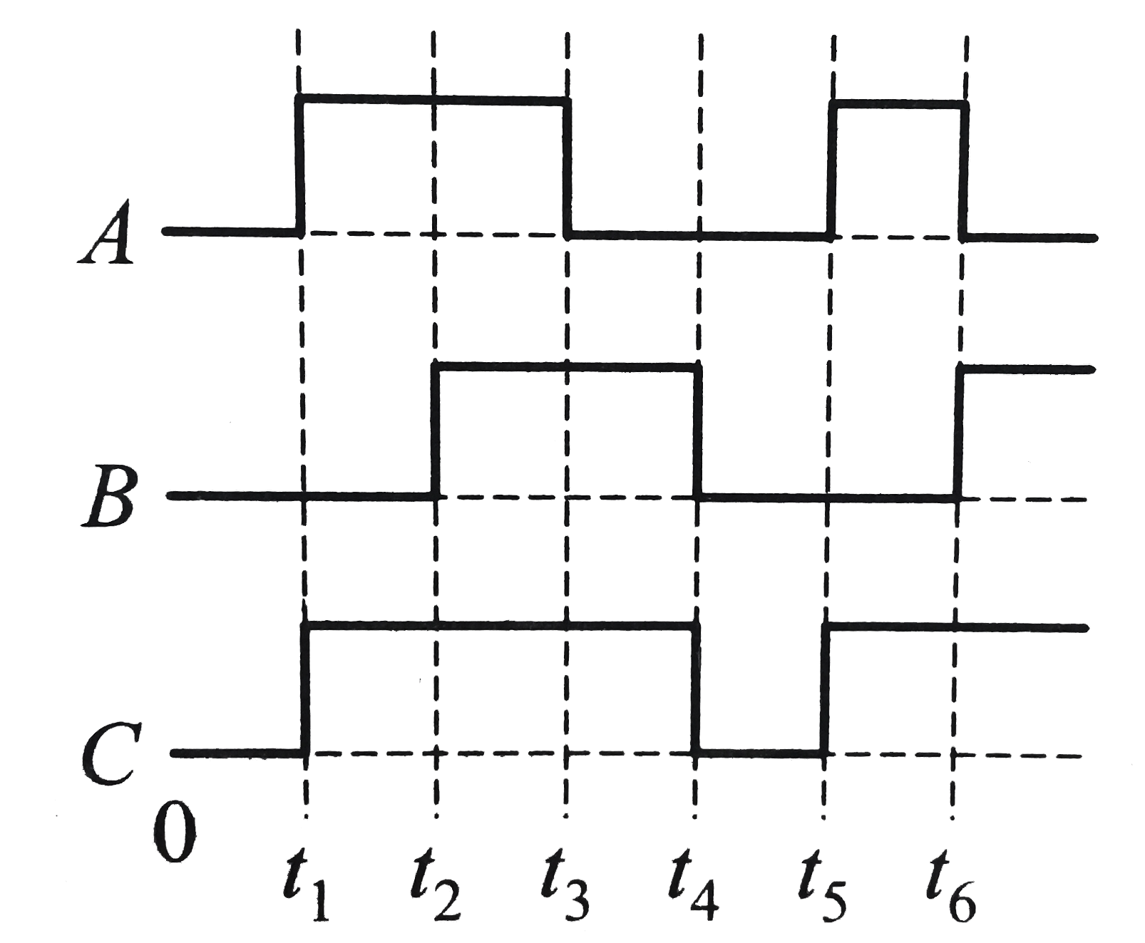
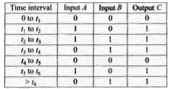
- The figure shows a logic circuit with two inputs A and B and the outpu...
Text Solution
|
- The input resistance of a silicon transistor is 100 Omega. Base curren...
Text Solution
|
- To get an output Y = 1 in given circuit, which of the following input ...
Text Solution
|
- In a common emitter (CE) amplifier having a voltage gain G, the transi...
Text Solution
|
- In a n-type semiconductor, which of the following statement is true?
Text Solution
|
- The output (X) of the logic circuit shown in figure will be
Text Solution
|
- The given graph represents V-I characteristic for a semiconductor devi...
Text Solution
|
- The barrier potential of a p-n junction depends on : (i) type of semic...
Text Solution
|
- Which logic gate is represented by the following combination of logic ...
Text Solution
|
- If in a p-n junction diode , a square input single of 10 V is applied...
Text Solution
|
- The input signal given to a CE amplifier having a voltage gain of 150 ...
Text Solution
|
- In the given figure, a diode D is connected to an external resistance ...
Text Solution
|
- To get output 1 for the following circuit, the correct choice for the ...
Text Solution
|
- A n-p-n transisitor is connected in common emitter configuration in a ...
Text Solution
|
- Consider the junction diode as ideal. The value of current flowing thr...
Text Solution
|
- For CE transistor amplifier, the audio signal voltage across the colle...
Text Solution
|
- The given circuit has two ideal diodes connected as show in the figure...
Text Solution
|
- What is the output Y in the following circuit, when all the three outp...
Text Solution
|