A
B
C
D
Text Solution
Verified by Experts
The correct Answer is:


Topper's Solved these Questions
SEMICONDUCTOR ELECTRONICS : MATERIALS , DEVICES AND SIMPLE CIRCUITS
NCERT FINGERTIPS ENGLISH|Exercise HOTS|8 VideosSEMICONDUCTOR ELECTRONICS : MATERIALS , DEVICES AND SIMPLE CIRCUITS
NCERT FINGERTIPS ENGLISH|Exercise NCERT|8 VideosRAY OPTICS AND OPTICAL INSTRUMENTS
NCERT FINGERTIPS ENGLISH|Exercise NCERT Exemplar|11 VideosWAVE OPTICS
NCERT FINGERTIPS ENGLISH|Exercise Assertion And Reason|15 Videos
Similar Questions
Explore conceptually related problems
NCERT FINGERTIPS ENGLISH-SEMICONDUCTOR ELECTRONICS : MATERIALS , DEVICES AND SIMPLE CIRCUITS -Assertion And Reason
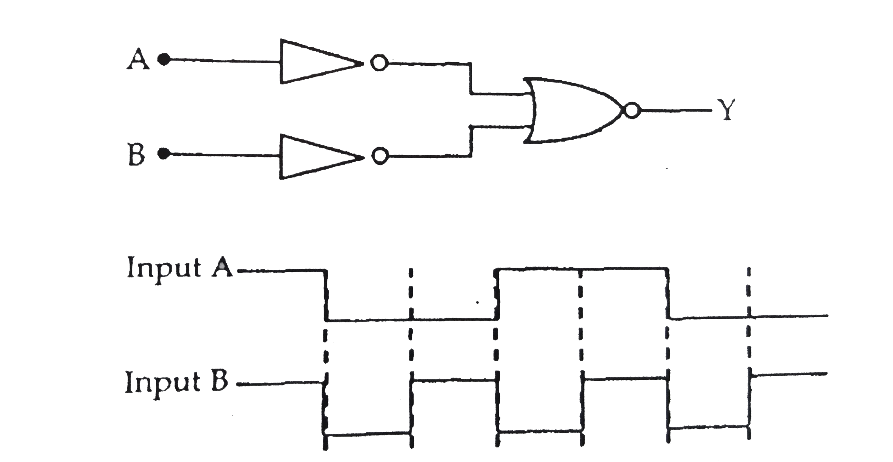
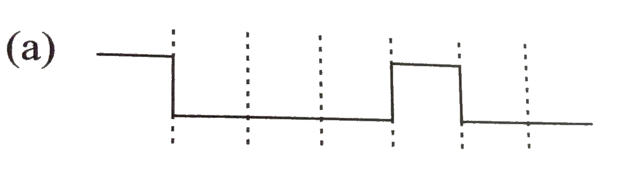
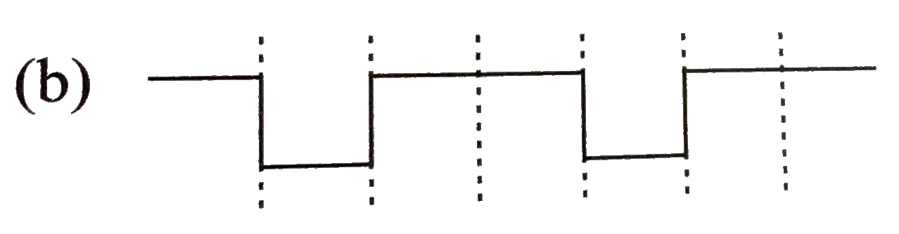
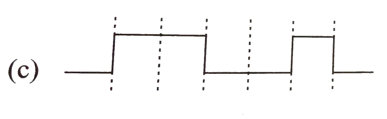
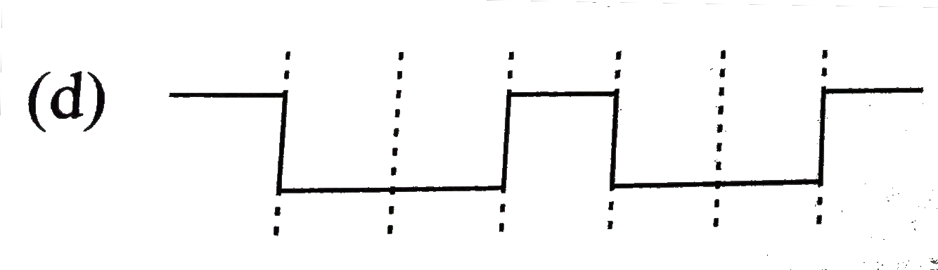
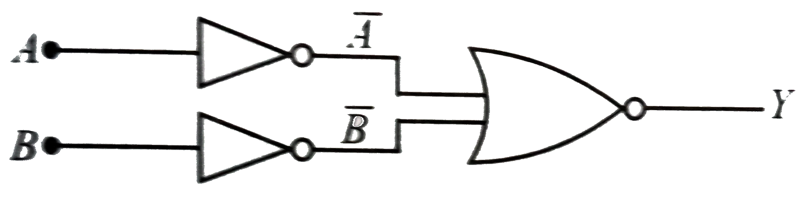
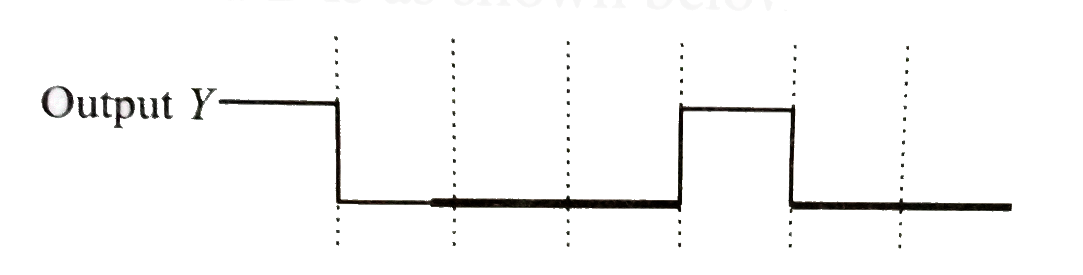
- The logic circuit shown below has the input waveforems 'A' and 'B' as ...
Text Solution
|
- Assertion: If there is some gap between the conduction band and the va...
Text Solution
|
- Assertion : The electrons in the conduction band have higher energy th...
Text Solution
|
- Assertion : In a semiconductor, the conduction electrons have a higher...
Text Solution
|
- Assertion: The probability of electrons to be found in the conduction ...
Text Solution
|
- Assertion: The conductivity of an intrinsic semiconductor depends on i...
Text Solution
|
- Assertion: The conductivity of an intrinsic semiconductor depends on i...
Text Solution
|
- Assertion: Thickness of depletion layer is fixed in all semiconductor ...
Text Solution
|
- Assertion: Zener diode works on aa principle of of breakdown voltage. ...
Text Solution
|
- Assertion : Zener diode is used to obtain voltage regulation Reason ...
Text Solution
|
- Assertion: The semiconductor used for fabrication of visible LEDs must...
Text Solution
|
- Assertion : In a transistor the base is made thin. Reason: A thin b...
Text Solution
|
- Assertion : Two p-n junction diodes placed back to back, will work as ...
Text Solution
|
- Assertion : In an oscillator, the feedback is in the same phase which ...
Text Solution
|
- Assertion : In an OR gate if any of the input is high, the output is h...
Text Solution
|
- Assertion: This circuit acts as OR Gate. Reason: Truth table for...
Text Solution
|