Home
Class 11
PHYSICS
in the foll. Circuit of PN junction , di...

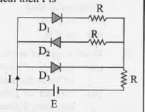
in the foll. Circuit of PN junction , diodes `D_1, D_2 and D_3` are ideal then I is

A

E/R

B

E/(2R)

C

(2E)/(3R)

D

ZERO

Text Solution

Verified by Experts

Promotional Banner

Topper's Solved these Questions

  • SCALARS AND VECTORS

    TARGET PUBLICATION|Exercise Evaluation Test|19 Videos
  • Sound

    TARGET PUBLICATION|Exercise Exercise|248 Videos

Similar Questions

Explore conceptually related problems

A PN junction diode can be used as a rectifier. Why ?

Three photo diods D_1 , D_2 and D_3 are made of semiconductors having band gaps of 2.5 eV, 2eV and 3eV, respectively. Which ones will able to detect light of wave length 6000 overset @(A) ?

The metal sheet shown in figure, with two holes cut of unequal diameters d_1 , and d_2 (d_1> d_2) . If the sheet is heated

Draw neat labelled circuit diagram using junction diodes as a full wave rectifier

consider the junction diode as ideal. The value of current flowin g through AB is

figure shows ttwo p-n junction diodes alond with aresistance R and a dc battery E. the path of flow of appreciable current in the circuit is,

With the help of neat circuit diagram, Explain working of p-n junction diode as a half-wave rectifier

the circuit has two oppositely connected ideal diodes in parallel. What is the curenet ideal dioddes in parallel. What is the current foll. In the circuit?

A pn junction diode in which light is allowed to fall on its junction is

for the current shiown in the figure . The equivalent resistance between A and B for two cases (i) V_A > V_B (ii) V_B> V_A is ___ ohm and ____ ohm ( D_1 and D_2 are ideal diodes)

TARGET PUBLICATION-SEMICONDUCTORS-EXERCISE
  1. in a semiconductor diode, a p-side is earthed and n-side is applied a...

    Text Solution

    |

  2. figure shows ttwo p-n junction diodes alond with aresistance R and a d...

    Text Solution

    |

  3. in the foll. Circuit of PN junction , diodes D1, D2 and D3 are ideal t...

    Text Solution

    |

  4. OF THE DIODES SHOWN IN the foll. Diagrams, which one is reverse biased...

    Text Solution

    |

  5. a semiconductorX is made by doping a germanium crytsal with arsenic (z...

    Text Solution

    |

  6. the dominant mecahnisms for motion of chargecarriers in forward and re...

    Text Solution

    |

  7. serious draback of the semiconductors devices is

    Text Solution

    |

  8. in LED, to avoid damage to the diode is used

    Text Solution

    |

  9. in LED, intensity of emitted light

    Text Solution

    |

  10. which of the foll. Is NOT an appliction of photodiode?

    Text Solution

    |

  11. in a p-n junction photo cell, the value of photo-electromotive force p...

    Text Solution

    |

  12. Assertion :light emitting diode (LED) emits spontaneous radiation reas...

    Text Solution

    |

  13. thermistors may have

    Text Solution

    |

  14. which of the foll. Graphs represents NTC thermistors

    Text Solution

    |

  15. the circuit has two oppositely connected ideal diodes in parallel. Wha...

    Text Solution

    |

  16. a p-n junction diode when forward biased has a drop of 0.4 V which is ...

    Text Solution

    |

  17. for a photodiode , the forbidden energy gap (E8)of the material used i...

    Text Solution

    |

  18. if the band gap between valence band and conduction band in a matereia...

    Text Solution

    |

  19. in insulatore (C.B. is conduction band and V.B. is a valence band)

    Text Solution

    |

  20. the energy gap in case of which of the foll. Is less than 3eV?

    Text Solution

    |